Abstract: In communication and control systems, asynchronous serial communication controllers (UARTs) are often used to realize the transmission of system auxiliary information. In order to achieve multi-point communication, software is usually used to identify the data sent to this site or other sites, which will increase the CPU overhead. An FPGA-based UART IP is introduced. The hardware implements the data filtering function during multi-point communication, which reduces the burden on the CPU and improves the system performance.
In communication and control systems, asynchronous serial communication is often used to achieve auxiliary communication between multiple boards, and each board is connected by a bus. In order to achieve point-to-point communication, a more complex communication protocol needs to be defined by the software to filter the data exchanged, which consumes more CPU time. The 89C51 single-chip microcomputer has a nine-bit communication method, which uses a single address bit to realize the selection of the communication object. Only the address sent to this address is interrupted to receive data. When a general-purpose UART chip such as 16C550 and 89C51 forms a bus-type communication system, the CPU needs to process the received address and generate nine-bit data through software. The UART introduced in this article is designed with Verilog HDL hardware description language, which can be implemented with FPGA and can be used in SoC design. Its main features are as follows: 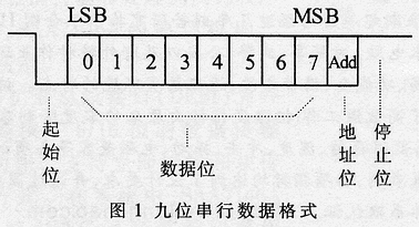
· Full hardware address recognition, filtering data without CPU intervention; supports a special address, which can be used for monitoring and broadcasting.
· Support two working modes: query and interrupt, interrupt programmable.
· The receiving and sending channels have 128Byte FIFO, each receiving byte is accompanied by status information.
· The design uses Verilog HDL language, full synchronous interface, and good portability.
· Support self-loop test function.
· The baud rate can be programmed to support eight or nine data formats.
The nine-bit serial data format of the designed UART is shown in Figure 1. In the idle state, the data line is in a high state. The bus jumps from high to low, the negative pulse with a width of one baud rate time is the start bit, and then the 8-bit data bit. After the data bit is the address information bit of lbit. If this bit is 1, it means that the transmitted byte is address information; if this bit is 0, the normal data information is transmitted. After the address indication bit is the stop bit of serial data.
1 UART design
UART adopts modular and hierarchical design ideas. All designs are implemented in Verilog HDL. Its composition block diagram is shown in Figure 2. The entire UART IP consists of a serial data sending module, a serial data receiving module, a receiving address recognition module, receiving and sending HIFO, bus interface logic, registers and control logic. The serial sending module and receiving complete the parallel / serial and serial / parallel conversion, and the identification of the receiving address is completed by the receiving address identification module. Send and receive HIFO is used to buffer the data sent and received. The bus interface logic is used to connect the UART IP internal bus and the HOST interface. 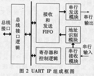 The registers and control logic implement all data transmission and reception, control and status registers, internal interrupt control and baud rate signal generation within the UART IP. The design principles of the main parts are explained in detail below.
1.1 Serial data transmission module
The serial data transmission module converts the data or address code from parallel to serial and outputs it from the serial bus. The design is implemented by finite state machine, which is divided into three states: idle, fetch and send. The state transition is shown in Figure 3. Each state is described as follows:
Idle state: The state machine continuously detects the transmit enable bit, UART enable bit, and transmit FIFO empty / full flag bit. If the enable bit is high, the UART enable is open and the FIFO empty flag bit is low, serial transmission enters the status.
Access state: In this state, the data or address to be sent is taken from the transmit FIFO in two cycles, and then enters the send state.
Sending state: In this state, the state machine sends the start bit, data bit, and address indication bit in sequence according to the nine-bit serial data format. After the stop bit is sent, it returns to the idle state. After one byte of data is sent, the next byte of data is sent.
1.2 Serial data receiving module
The serial data receiving module is used to detect the start bit of serial data, convert the serial data on the serial bus into parallel data and output it. The receiving logic is also implemented by finite state machine, which is divided into four states: idle state, looking for start bit, receiving data and saving data. The state transition diagram is shown in Figure 4. Each state is described as follows:
Idle state: In this state, the status of receive enable, UART enable, and serial input signal is continuously detected. If the serial input signal changes from high to low and the UART enable and receive enable are both high, the sample counter is reset and the state of finding the start bit is entered. 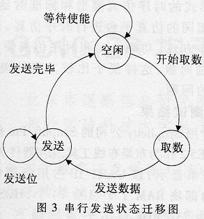
Looking for the start bit: In this state, the state machine waits for half a baud rate, and then re-detects the level of the serial input. If it is low, it judges that the received start bit is valid and enters the received data state; otherwise, it is considered that there is interference on the data bus, the start bit is invalid, and returns to the idle state again.
Receiving data: In this state, the data bits, address indication bits, and stop bits of the serial data line are received in sequence, and the data storage state is entered after the end.
Save data: This state outputs the received serial data from the parallel bus of the interface in parallel, and then returns to the idle state, ready to search and receive the next byte of data.
In order to improve the resistance to sudden interference on the serial input, for the received data, the sample is continuously sampled three times in the middle of the pulse, and more levels are used as the received valid data. The sampling frequency of all received data is 16 times the received baud rate.
1.3 Hardware address recognition module
The hardware address recognition module is used to determine the address and data from the received data. When the address recognition function is turned on, the data is passed or discarded; when the function is turned off, all data will pass. The address recognition module is a finite state machine with two states, divided into address and data states. The state transition diagram is shown in Figure 5. The status description is as follows:
Address status: In this status, judge the received data and the address recognition enable bit. If the address recognition function is not turned on, any address received will enter the data state. If the address recognition function is turned on, the received address is compared with the local address. If they are equal, the address is saved and the data state is entered; otherwise, the data and address continue to be received in this state, and the received data is ignored.
Data status: output the received data until the address bit is received, return to the address status, and process the address.
In order to realize the monitoring and broadcasting functions, the address 255 is used as a special address, which can be matched with any address. If the address of this station is 255, this station can receive data from any address. This function can be used to monitor the data on the bus; if the destination address of the sent data is 255, any station will receive this data, this function can be used Used to send broadcast data.
1.4 FIFO design 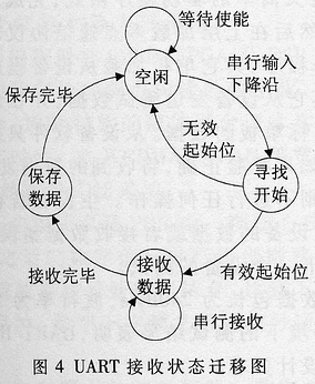
The FIFO is composed of control logic and dual-port RAM. The control logic is used to realize the function of converting a dual-port RAM into two FIFOs. These two FIFOs are used to send and receive data buffers respectively; interrupt control is used when interrupting the working mode. Manage the interrupt status and control information inside the UART.
In order to reduce the number of required block RAMs, the receive and transmit FIFOs are implemented using the same block RAM, and the arbitration mechanism is used to ensure that the four ports of the two FIFOs have only two operations at the same time, which does not affect the reading and writing of the FIFO.
1.5 Bus interface
The UART uses a synchronous interface. All signals are sampled at the rising edge of the system clock, and the device's handshake is completed with a one-bit response signal.
The width of the data bus is 8 + 2. When connected to a 16-bit or 32-bit data bus, the data and address indication bits of the received data can be read at one time to reduce the number of bus operations; if connected to an 8-bit system, only the lower 8-bit data lines can be connected to receive data Address information can be read through the internal status register.
1.6 Registers and control logic
The register part realizes the sending, receiving, controlling and status registration of all the data inside the UART. It is used to set the data format, sending and receiving baud rate, FIFO control, local address, address recognition, interrupt control and status registration of the UART, so as to control the work of the UART.
The control logic generates all required baud rate signals and corresponding rising and falling edge indication signals, and outputs corresponding signals synchronized with the system clock according to the baud rate selected for actual work. The block diagram of the baud rate generation logic is shown in Figure 6.
2 Functional and timing simulation
First, the simulation platform of the functional simulation design system is combined. The simulation platform is shown in Figure 7. The system simulation platform and simulation incentive are designed in VerilogHDL language, which can be used for both functional simulation and timing simulation, but not for the synthesis of both. The register-level model is an RTL description for UART IP design, 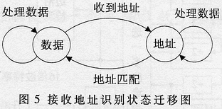 All are written in Verilog HDL statements that can be synthesized. The software used for the simulation is ModelSim.
Functional simulation includes the following aspects:
(1) Simulation of basic module connection timing. Firstly, the UART interface model is designed in a descriptive way, and the simulation excitation is used for simple read and write operations, and the simulation excitation signal and system simulation platform are designed. Then, the design of each sub-module of the UART is gradually completed in combination with the simulated excitation signal. During simulation, it is necessary to gradually observe the waveform of the UART interface signal, the interface signal waveform of the UART internal module, the state transition of various state machines, the value of the data pointer and the value of the status bit, and gradually complete the UART design of the register transmission level.
(2) Work simulation of UART. After completing the register transfer level model of RTL, according to the mode of the system software, HDL is used to design a simulation incentive for data transmission and reception, open the self-loop function, and send and receive data. Simulation can be divided into two working modes: simulation query and interrupt. For the interrupt working mode, the interrupt mechanism of software needs to be simulated in HDL language,
Carry out the simulation of interrupt working mode. Finally, open the address recognition function, send data of different destination addresses, and observe the hardware address recognition of the UART.
After the functional simulation is completed, the design is placed and routed to generate a timing simulation model and standard delay file in the form of Ver-ilog HDL, and timing simulation is performed using the same simulation platform as the functional simulation. Timing simulation only needs the simulation working mode. Functional simulation and timing simulation use the same simulation platform and excitation vector, which makes it easy to compare the differences between the two and find problems in the design code. 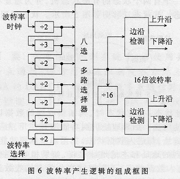
3 Synthesis and test results
This design uses Synplicity Pro's Synplify Pro as a comprehensive tool, Xilinx ISE5.2 as a place and route tool, and the device used is XC2S100IIE-7. The comprehensive results show that the resource occupied by the UART IP is: 275 SLICE, 1 internal block RAM, 24 I / O, and the frequency that the HOST bus can reach is 73.2MHz.
The test procedure refers to the generation of simulation stimulus and is designed in C language under vxWorks operating system. The method used for testing is exactly the same as the work simulation, except that the simulation stimulus corresponds to the test program, and the RTL model corresponds to the actual FP-GA device.
The multi-point test uses five boards, uses half-duplex bus mode, defines a simple data packet format, and is used to detect data errors and return data. The format of the data packet is the beginning of the address, followed by the maximum data of 255Byte; the data part includes the address of the sender, the data checksum and the length of the packet. In addition, a simple driver format is defined to complete the sending and receiving and control of basic data, and then the multipoint communication protocol is loaded on the upper layer. One of them loads the master device program, and the other boards load the slave device program. The master device periodically sends test data to other slave devices and waits for receiving data from the target board within a specified time. The slave device software only receives the data sent to the board. If the verification is correct, the received data is sent to the master device; if there is an error, no operation is performed. If the master device fails to receive data from the slave device within a specified time or receives data incorrectly, it determines that the communication is abnormal and performs the next device test. 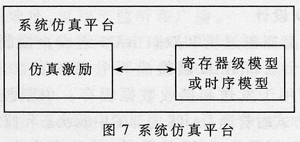
During the test, the data packet length is 240Byte and the baud rate is 115200. The test results under normal temperature and high and low temperature environments show that the UART IP works stably and reliably and meets the design requirements.
This UART IP is all designed with Verilog HDL. It can be used as a system multi-point communication controller in the communication and control system implemented by FPGA, and can also be used in the design of system on chip (SoC). When used for multipoint communication, it can effectively reduce the extra load of the CPU and improve the utilization rate of the CPU system. Due to the language description and strong portability, it can be used in FPGA chips of different manufacturers and different models, which improves the design speed and efficiency of the system.
Liquid Crystal Display For Home Appliances
Liquid Crystal Display For Home Appliances,High Resolution Portable Lcd Display,Refrigerator Lcd Liquid Crystal Display,Response Fast Remote Lcd Monitor
Dongguan Yijia Optoelectronics Co., Ltd. , https://www.everbestlcdlcm.com