Design and Implementation of Digital Communication Signal Generator Based on ADSP-BF533
0 Preface
In the research of communication confrontation, in order to simulate the real digital communication signal scene, the digital communication signal generator is an indispensable instrument. The communication signal generators on the market are very expensive and the functions are relatively simple. Moreover, the output symbols of this type of communication signal generator are uncontrollable, and the signal-to-noise ratio and interference-to-signal ratio cannot be adjusted dynamically. Therefore, it is impossible to simulate a mixed environment of multiple modulation types of communication signals. inconvenient. Therefore, it is of great theoretical significance and practical value to carry out research work on reconstruction methods of high-precision communication signals and noise interference waveforms.
1 Introduction to ADSP-BF533 chip
ADSP-BF533 is a medium-to-high performance product of the Blackfin series, which is specifically aimed at various applications in multimedia (especially video processing) and communications. It contains 2 multipliers / accumulators (MAC), 2 40-bit ALUs, 4 video ALUs and 1 40-bit shifter. The working clock of BF533 core can be up to 600 MHz. The arithmetic unit processes 8-bit, 16-bit or 32-bit data from the register bank.
Each MAC of BF533 can complete a 16-bit by 16-bit multiplication operation per cycle, and can accumulate the result into a 40-bit accumulator, while providing 8-bit precision expansion. The ALU unit performs standard arithmetic and logical operations. The two ALUs can handle 16 or 32-bit data. The arithmetic unit has great flexibility. Therefore, it can meet the requirements of signal processing in various applications.
ADSP-BF533 regards memory as a unified 4GBytes address space. All resources, including internal memory, external memory, and I / O control registers, occupy corresponding parts of the common address space and are independent of each other. The memory of each part of this address space is arranged in a hierarchical structure to provide a high-performance price ratio. High-speed, low-latency, small-capacity memory (such as CACHE or SRAM) is located very close to the processor, while low-speed, high-latency, large-capacity, low-cost memory (such as SDRAM or Flash) is far from the processor.
The L1 memory in the BF533 is the highest performance and most important memory in the core; the L2 memory is used to provide additional storage capacity, and the performance is lower: the off-chip storage system is accessed through the external bus interface unit (EBIU); the asynchronous memory unit can be connected 4 Asynchronous memory bank or IO interface, each bank can support a maximum of 1MBytes physical addressing space; synchronous memory unit can be expanded by SDRAM, can access up to 128MBytes of physical storage space; memory DMA controller provides high-bandwidth data The transmission ability can complete the block transmission of code or data between the internal L1 / L2 memory and the external memory space.
In addition, ADSP-BF533 also provides a parallel interface (PPI) that can be directly connected to parallel A / D and D / A converters, ITU-656-compliant video encoders and decoders, and other general-purpose peripherals. PPI includes a dedicated clock pin, up to 3 frame synchronization pins and up to 16 data pins. The general mode of PPI is divided into four main working modes, namely: data reception for signal generation in frame synchronization internally, data reception for frame synchronization signal externally generated, data transmission for frame synchronization signal internally generated, data for frame synchronization signal externally generated send. Each PPI_CLK clock cycle can transmit up to 16 bits of data, which is widely used in various data collection and data transmission occasions.
2 System hardware design
The digital communication signal generator system is divided into two major modules: a microcomputer module and a waveform generation module. The microcomputer is a general-purpose computer or PC, and the waveform generation module is a designed signal generation board. Figure 1 shows the overall block diagram of the system. 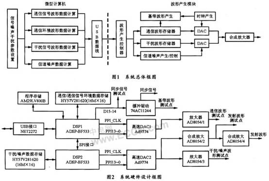
The general microcomputer first based on the parameters input by the user. Generate various types of digital modulation signals and Gaussian narrow-band white noise and various types of interference signals, and then transfer the data to the signal generation board through the USB interface. The signal generation board then cyclically takes out the data in the communication waveform memory and interference / noise memory through the waveform generation controller, and finally generates a continuous digital communication signal waveform through the DAC. Figure 2 shows the block diagram of the system hardware design.
DSP1 in the hardware design is the core of the entire system, which can directly communicate with the microcomputer and control the loading and running of DSP2. The loading mode of DSP1 is BMODE 01, which is loaded from external Flash; DSP2 is BMODE 10, which is loaded through the SlaveSPI interface.
DSP1 first receives the waveform data packet transmitted by the microcomputer through the USB interface, and transmits the communication waveform or the communication environment waveform data in the data packet to the communication / communication signal environment waveform data memory (SDRAM1) by MDMA. At the same time, the noise data is transferred to the internal RAM of DSP2 in SPI MDA mode, and then after DSP2 is received, the noise / interference data is stored in the noise / interference data storage section (SDRAM2) in MDMA mode. DSP1 transmits the signal-to-noise ratio / interference-to-signal ratio parameters to the internal RAM of DSP2 through SPI non-DMA. The high bit (D15) of the communication data is the baseband code stream data, and D14 is the synchronization signal, which is used to test the baseband code stream.
In the system, the sampling frequency of all waveform parameters is 10MHz, the data capacity is 16 M × 16 bits, and waveform data of 1.5 seconds can be stored. The effective number of data is 14 digits. DSP1 directly reads the communication waveform data from SDRAM1 through PPIDMA and transmits it to DAC1 to generate communication waveform. DSP2 uses the program to generate random addresses to get the starting address of MDAM0, and then reads the stored noise waveform data from SDRAM2 into DSP2 internal RAM, and performs amplitude weighting in the internal RAM according to the signal-to-noise ratio, and then transfers to PPI DMA DAC2, generates a noise waveform. If the interference signal is included, DSP2 needs to read the interference data into the internal RAM through MD-MAl, and weight the amplitude in the internal RAM according to the signal-to-signal ratio, then superimpose it with noise, and then output it to DAC2 through PPI DMA to generate interference and noise. Mixed waveforms. The PPI clock PPI_CLK signal is generated by the timer of each DSP.
The number of bits of the two DACs is 14 bits, and is set to a 4-fold interpolation mode, that is, the DAC input data rate is 10 MSPS, and the output conversion rate is 40 MSPS. The clock required for DAC conversion is shared with PPI_CLK, and the DAC is connected to the lower 14 bits PPI13 ~ PPI0 of the BF533PPI bus. The baseband code stream is output through the PPI15 pin of DSP1, and the synchronization signal is output through the PPI14 pin of DSP1, and the output waveform is driven through 74AC11244.
The analog signal output by the DAC is buffered and amplified by the AD8054, and then it is divided into two channels after signal and noise synthesis, which can be used as a test waveform and signal source.
If you need to simulate the communication signal environment, you need to calculate the superimposed data of multiple signals in the microcomputer and then transfer it to the communication / communication signal environment data memory (SDRAM1). The other processes are the same as the communication method. In this mode, the baseband stream cannot be tested, but the sync signal can still be tested.
3 System software design
The microcomputer in the system adopts Windows 2000 / XP operating system, its USB driver program is developed by DDK, and the control application program can be developed through VS2005. The computer can generate 2ASK, 2FSK, 8FSK, 2PSK, 2DPSK, QPSK, QDPSK and other communication environment signals according to the input parameters of the user, or a mixture of several of them. Related interference signals. The data can be packaged and sent to the signal generation board through the USB interface. Subsequently, the computer processes the data by sending control command words, mainly to start outputting the waveform, stop outputting the waveform, update the waveform data, update the communication signal environment waveform data, update the interference / noise data, and update the signal-to-noise ratio or dry-signal ratio.
The software design of the system is mainly for BF533 programming. Blackfin series DSP supports C language and assembly language in software, and supports mixed programming of both. The C language program has a good structure, strong readability, and easy portability, but the processing speed for interrupts is slow. Assembly language has a fast processing speed but poor readability and is not easy to debug. C and assembly mixed programming combine their respective advantages, can construct a program with good structure and fast execution speed. The software program flow chart of this system is shown in Figure 3. In addition, during the programming process, pay attention to the following items:
(1) Whether using C or assembly, there is only one set of identical registers available in the system, so to use these registers, the sub-function must be saved first and restored before returning.
(2) It should be used strictly according to the type of register, and different types of registers cannot be mixed.
(3) Try to save register resources.
(4) In order to improve the speed of code running, it is necessary to be good at using parallel instructions.
In this system, the interrupt and DMA methods are used more, mainly using PF interrupt, MDMA interrupt, SPI DMA interrupt and PPI DMA interrupt. The system interrupt controller can control all system interrupts and manage their priority. DMA does not require the core to participate, and the core can be used for calculations or to respond to interrupts during DMA operation.
After the system is powered on, DSP1 first reads its own loading code from Flash, then reads the loading code of DSP2 from Flash and transmits it to DSP2 through SPI interface to load DSP2, and finally initializes the system clock, SDRAM, NET2272USB control chip, enter Wait for the computer user's instruction status. 4
4 Conclusion
The digital communication signal generator only needs to be installed on a general-purpose microcomputer or PC to achieve software. Its low cost, high efficiency, and good real-time performance, especially in the simulation of communication countermeasure signal sources, it shows unparalleled superiority. Sex.
10 inch tablet is the most important size on tablet market. Which kind of clients like more? The answer is loving bigger size or storage, longer working time, etc. Since Android Tablet 10 inch is usually equipped with full HD screen, memory support up to 8GB, storage up to 256GB, battery up to 7000mAh-working 5-8hours. However, 8 inch android tablet mainly up to 4GB ram 64GB ROM, 4000mAh battery. At this store, you can see more than ten different 10 inch tablets on sale and one 10 inch windows tablet with magnetic keyboard option, and high level CPU and SIM Card option. Besides, you can also see amazon tablet 10 inch with competitive cost, especially take above 1000pcs. Except android tablet, 14 inch 64Gb Student Laptop for online learning, 15.6 inch celeron n5095 business laptop, 15 inch intel i3, i5, i7 10th or 11th generation Gaming Laptop and 16 inch laptop with 4gb graphics card and 16gb ram 512GB ssd alternatives also.
Any other special requirements, just fee free to contact us. Will try our best to support you.
10 Inch Tablet,10 Inch Tablets On Sale,Android Tablet 10 Inch,Amazon Tablet 10 Inch,10 Inch Windows Tablet
Henan Shuyi Electronics Co., Ltd. , https://www.shuyitablet.com