
Micro-interview: Joseph Montanya i Silvestre, CEO of Nanusens
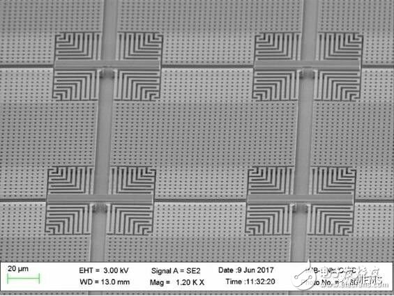
According to James Consulting, NANUSENS' NEMS (Nano Electro Mechanical Systems) sensors are manufactured using standard CMOS processes and masking techniques. In the process of NANUSENS, HF vapor (vHF) is used to etch the inter-metal dielectric (IMD) through the pad openings in the passivation layer to obtain the sensing structure of the nanosensor. The holes are then sealed and the chip is packaged as needed. Because the sensor uses only standard CMOS processes and can be directly integrated with the active circuitry required, this sensor can achieve the same high yield as CMOS devices. Nanusens claims that their solution reduces sensor design size by an order of magnitude, from a linear feature size of MEMS (Micro Electro Mechanical Systems) devices from 1 to 2 um to a 0.3 um NEMS. This reduces the surface area of ​​the device microstructure by two orders of magnitude from two dimensions, thereby significantly reducing microscopic attraction and solving the adhesion problems faced by MEMS inertial sensors. Recently, we had the opportunity to interview Mr. Josep Montanyà i Silvestre, CEO of Nanusens. Q: What technology are you studying? Why choose this technical solution? Josep Montanya i Silvestre: We are developing inertial sensors. Our technology can produce many different types of NEMS devices in a CMOS process. We chose to start with inertial sensors for two main reasons. First, because of the previous research results of Baolab Microsystems and the subsequent inertial sensor research conducted by UPC (Catalonia Polytechnic University), we continued to develop on the basis of these research work. Another reason is that we recognize that if we can provide what our customers have been pursuing – low cost or high performance – this will be a good business opportunity. Currently, we are developing in these two directions. We are currently developing the fastest-growing device at a lower cost, and we will be the first to bring it to market. After that, we will develop higher performance products. After that, we will continue to develop NEMS devices other than inertial sensors. Essentially, our technology can make devices using CMOS processes, which makes our market more responsive.
NEMS Motion Sensor Q developed by Nanusens : Can you tell us more about the origin of your technology? Josep Montanya i Silvestre: Our technology is derived from the research accumulated by Boalab Microsystems over the past 10 years. The company closed down in 2014 due to certain strategic decision-making issues. The core staff team later founded Nanusens.
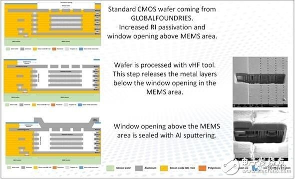
Nanusens CMOS NEMS Manufacturing Process Q: Please tell us about your current financing situation? Josep Montanya i Silvestre: Nanusens has completed a $2.1 million financing from Inveready and Caixa Capital Risc from Barcelona (Barcelona), including Dieco Capital from the Netherlands. As I mentioned earlier, Nanusens has benefited from all previous research by Baolab Microsystems, and Baolab Microsystems has raised $12 million before the closure. Q: What are the main challenges you are currently facing? Josep Montanya i Silvestre: Our main challenge is to complete product development in accordance with financing requirements and quickly expand the market. Our current investors have given full support and completed a new round of financing. However, they are seed round financing, so there are many restrictions on the amount of investment. We have already pushed the first product to the market in accordance with financing requirements. We are currently seeking new investments to accelerate the development of this and other new products to avoid potential opportunities delays. Q: What is your company's vision? How will it develop in the next 5 to 10 years? Josep Montanya i Silvestre: Our company's vision is to create new standards for a wide range of MEMS sensors. They need to move from MEMS to NEMS, from micron to nanoscale, for better device performance and reliability. Moreover, they need to switch from their respective processes to standard CMOS processes to achieve mass production cost advantages, faster time to market, and higher throughput and second source of supply. Q: What is your product plan for this year? Key milestones in 2018 include? Josep Montanya i Silvestre: The first milestone in 2018 is the launch of our first inertial sensor product, which is expected to be in the second quarter of 2018. In addition, we plan to complete a new round of financing in late 2017 or early 2018 to help us further accelerate development and reduce the risk of delaying market opportunities. Q: Are you looking for an industrial partner now? If so, what types of partners do you need? Josep Montanya i Silvestre: We are a Fabless semiconductor company. Our supply chain is very clear. Starting with GLOBAL FOUNDRIES, they offer CMOS foundry services, and finally distributors from China, such as EDOM. They are top partners. Not only that, although our technology already has many user stories and applications, we will continue to develop partners, cooperate with other semiconductor companies that want to use our technology to solve specific applications, or make strategic investments, or establish joint development partnerships. Our nanosensors are fabricated in CMOS technology and can be embedded in all CMOS ICs. This will bring more possibilities, and this is not something we can do alone.
GPS Tracker, locator for all vehicles
Features that already exist
âš« Tracking: It sends GPS (Location, speed) and sensors (if any) information to your application server with configurable report interval (moving or stationary).
âš« Geofence: It supports circle and polygon setting
âš« Backup Battery (optional): With a backup battery (300mAh), the device sends a tamper message if the main power supply harness is disconnecte
âš« Over Speed Limit: Reports over-speed limit.
âš« 3-Axis Accelerometer: With a built-in 3-axis accelerometer, the device can detect trip start/trip end, and to report harsh braking, harsh acceleration, and impact.
âš« Storing Message: The device stores up to hundreds of messages while there is no GSM signal.
âš« Low Voltage Detection (optional): Device switches to deep sleep mode if supply voltage drops below a threshold.
âš« Power Saving Mode: Device periodically wakes up and sleeps when vehicle engine is OFF.
âš« Expand other peripherals: Plenty of IOs, UARTs and AD to accomplish custom`s requirement.
âš« OTA (Over the Air): The device`s firmware can be upgraded via TCP.
âš« Waterproof Case: IPX65 waterproof.
âš« Bluetooth-positioning: It will support bluetooth feature for positioning.
âš« Mileage: Reports trip start, trip end and the mileage.
âš« CAN Communication: It can read VIN, RPM and many other standard
vehicle parameters via CAN BUS.
âš« GPIO and UART: The device has 5 configurable IOs. It can be
configured as 3 digital inputs, 2 digital outputs; 2 digital input, 1
analog input and 2 digital outputs; 1 digital input, 1 analog input, 1
digital output and 1 UART. These IOs can be used for engine starter
on/off detection, immobilization of engine starter, door lock, and for
connecting to various types of sensors.
Other functions can be customized
Vehicle GPS Trackers,Car GPS Trackers,Fleet management,LTE Vehicle GPS Trackers,LTE Car GPS Trackers
eSky wireless Inc , https://www.eskygpsiot.com