Most electronic systems now support hot-swap function. The so-called hot plugging, that is, when the system is working normally, the power is plugged and unplugged to a certain unit of the system without any impact on the system.
There are two main aspects to the impact of hot swapping on the system:
First, when hot plugging, the mechanical contacts of the connector will bounce at the moment of contact, causing the power supply to oscillate, as shown in the following figure:

This oscillation process can cause the system power supply to fall, causing bit errors, or system restart, which may also cause the connector to catch fire and cause a fire.
The solution is to delay the power-on time of the connector. During the ten milliseconds of the connector jitter ((t1 to t2), the connector is not energized. After the insertion is stabilized (after t2), the power is turned on again, that is, the anti-jitter delay. .
Second, when hot plugging, due to the charging effect of the large-capacity storage capacitor of the system, a large inrush current will appear in the system. As we all know, when the capacitor is charging, the current decreases exponentially (bottom left), so At the beginning of charging, the inrush current is very large.
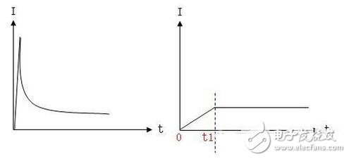
This inrush current may burn the equipment power fuse, so the inrush current must be controlled during hot plugging, so that it changes according to the ideal trend. As shown in the upper right figure, 0~t1 in the figure is the power slow start time.
In summary, the main function of the slow-start circuit is to achieve two functions:
1). Anti-shake delay power-on;
2). Controls the rising slope and amplitude of the input current.
There are two types of slow start circuits: voltage slope type and current slope type.
The voltage slope type slow start circuit has a simple structure, but the change of the output current is greatly affected by the load impedance, and the output current change of the current slope type slow start circuit is not affected by the load, but the circuit structure is complicated.
The following focuses on the voltage type slow start circuit.
MOS tubes are often used in designs to design slow-start circuits. The MOS transistor has a low on-resistance Rds and a simple driving function, and a small number of components can be used around to form a slow start circuit. Normally, PMOS is used in the positive power supply and NMOS is used in the negative power supply.
The following figure shows a -48V power supply slow-start circuit built with NMOS. Let's analyze the working principle of the slow-start circuit.
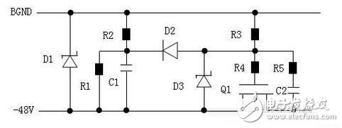
1). D1 is a clamp diode to prevent the input voltage from being too large to damage the rear stage circuit;
2) The role of R2 and C1 is to realize the anti-jitter delay function. In practical applications, R2 is generally selected as 20K ohms, and C1 is selected as 4.7uF;
3) The role of R1 is to provide a fast discharge channel for C1, which requires that the voltage divider value of R1 is greater than the voltage regulator value of D3. In practical applications, R1 is generally selected to be about 10K;
4). R3 and C2 are used to control the rising slope of the power-on current. In practical applications, R3 is generally selected to be about 200K ohms, and C2 is taken as 10 nF to 100nF;
5). The role of R4 and R5 is to prevent self-oscillation of MOS tube, requiring R4, R5lt;
6). The function of the clamp diode D3 is to protect the gate-source of the MOS transistor Q1 from being broken by high voltage; the function of D2 is to form an anti-jitter delay circuit composed of R2 and C1 and R3 and C2 after the MOS transistor is turned on. The power-on slope control circuit is isolated to prevent the MOS gate charging process from being affected by C1.
Let's analyze the slow start principle of the circuit:
Assume that the parasitic capacitance between the gate-source of the MOS transistor Q1 is Cgs, the parasitic capacitance between the gate and the drain is Cgd, the parasitic capacitance between the drain and the source is Cds, and the capacitance of the gate-drain is connected in parallel with the capacitor C2 (C2gt; 》Cgd), so the total capacitance of the gate-drain C'gd=C2+ Cgd, since the capacitance of Cgd is almost negligible relative to C2, C'gd≈C2, the turn-on voltage of the gate of the MOS transistor is Vth, during normal operation, the gate voltage of the MOS transistor is Vw (this voltage is equal to the clamping voltage of the Zener diode D3), and the time constant of the charging of the capacitor C1 is t=(R1//R2//R3)C1, since R3 is usually R1 and R2 are much larger, so t≈(R1//R2)C1.
The following three stages are used to analyze the working principle of the above voltage slow start circuit:
The first stage: -48V power supply charges C1, the charging formula is as follows.
Uc=48*R1/(R1+R2)[1-exp(-T/t)], where T is the time when the voltage of the capacitor C1 rises to Uc, and the time constant t=(R1//R2)C1. Therefore, the time required from power-on to MOS transistor turn-on is: Tth=-t*ln[1-(Uc*(R1+R2)/(48*R1))]
The second stage: after the MOS transistor is turned on, the drain current begins to increase, and the rate of change is proportional to the transconductance of the MOS tube and the rate of change of the gate-source voltage. The specific relationship is: dIdrain/dt = gfm *dVgs/dt, where gfm The transconductance of the MOS transistor is a fixed value, Idrain is the drain current, and Vgs is the gate-source voltage of the MOS transistor. During this period, the gate-source voltage is constant control of the drain-source current, and the MOS transistor is classified into a voltage-controlled type. The device is also derived from this.
The third stage: When the drain-source current Idrain reaches the maximum load current, the drain-source voltage also saturates. At the same time, the gate-source voltage enters the plateau period, and the voltage amplitude is Vplt. Since the drain-source current Ids remains constant during this time, the gate-source voltage Vplt=Vth+(Ids/gfm), and the gate current is Ig due to the fixed gate-source voltage causing the gate current to pass through the feedback capacitor C'gd. = (Vw-Vplt) / (R3 + R5), since R5 is negligible with respect to R3, Ig≈(Vw-Vplt)/R3. Since the gate current Ig ≈ Icgd, Icgd=Cgd*dVgd/dt. Since the gate-source voltage remains constant during this period of time, the rate of change of the gate-source voltage and the drain-source voltage is equal. Therefore, there are: dVds/dt=dVgd /dt=(Vw-Vplt)/(R3*C2).
It can be known from this formula that the slope of the drain-source voltage change is related to the value of R3*C2. For a system with a constant load, as long as the value of R3*C2 is controlled, the rising slope of the hot-swap surge current can be controlled.
The schematic diagram of the variation of the gate-source voltage Vgs, the drain-source voltage Vds, and the drain-source current Ids in the slow start phase is as follows.
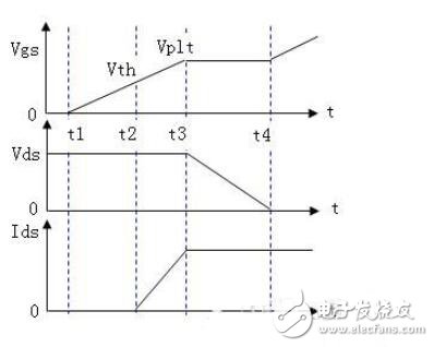
In the 0~t1 phase, the Schottky diode D2 is not yet turned on, so Vgs is equal to 0. During this time, the -48V power supply charges C2 through R3 and R5, and the voltage of C2 rises to the turn-on voltage of D2, MOS tube. The gate voltage starts to rise. When the gate-source voltage rises to the turn-on voltage Vth of the MOS transistor, the MOS transistor is turned on, and the drain-source current Ids starts to increase. When the gate-source voltage of the MOS transistor rises to the platform voltage Vplt. The drain-source current Ids also reaches a maximum. At this time, the drain-source voltage Vds enters saturation and starts to fall. When the platform voltage Vplt ends, the MOS transistor is completely turned on, the drain-source voltage is minimized, and the on-resistance Rds of the MOS transistor is minimized.
Steel Power Pole, Stainless Steel Power Pole, Steel Tapered Power Pole, Galvanized Steel Power Pole
YIXING FUTAO METAL STRUCTURAL UNIT CO.,LTD( YIXING HONGSHENGYUAN ELECTRIC POWER FACILITIES CO.,LTD.) , https://www.chinasteelpole.com