**Introduction**
Wireless communication networks are evolving rapidly, driven by the increasing demand for enhanced data services and higher bandwidth usage. Next-generation wireless systems must deliver faster data rates, lower power consumption, and greater reliability—goals that often conflict with one another. To address these challenges, a digital-to-analog converter (DAC) solution with high sampling rates, wide signal bandwidth, and excellent efficiency is essential. Modern high-speed DACs, such as those with GSPS sampling rates, offer multi-carrier GSM compatibility for multi-band, multi-standard radio base stations while reducing overall system power consumption and thermal density. This article explores how high-speed converters enable system designers to push the boundaries of innovation in wireless communication systems, achieving higher sampling rates, broader data bandwidth, and lower power consumption.
**High-Bandwidth Challenges in the System**
It is not uncommon for modern mobile base stations to support transmission bandwidths exceeding 300 MHz. As the need for wider data bandwidths and digital pre-distortion (DPD) technologies grows, the requirements for signal bandwidth and dynamic performance in high-speed DACs have also increased. Achieving higher system bandwidth presents three major challenges.
First, higher signal bandwidths require faster DAC sampling rates. According to the Nyquist-Shannon sampling theorem, the sampling rate should be at least twice the frequency of the signal being synthesized. Therefore, without considering other constraints, the DAC sampling rate must increase proportionally with the signal bandwidth. Additionally, analog reconstruction filtering plays a critical role in system design. A higher DAC sampling rate simplifies filter design by allowing for a more manageable transition band between the target signal and unwanted image frequencies. For example, if a signal has a bandwidth of ±50 MHz at a center frequency of 150 MHz, the DAC output reaches up to 200 MHz. In contrast, a signal with a bandwidth of ±150 MHz at 300 MHz requires the DAC to reach 450 MHz, demonstrating the need for significantly higher sampling rates.
Second, higher signal bandwidths demand faster and more reliable data interfaces. The required throughput increases proportionally with the signal bandwidth. For instance, achieving a 300 MHz system bandwidth using IQ modulation requires a dual DAC input data rate of 750 MSPS (assuming a filter roll-off factor of 0.2). This results in an input data period of just 1.33 ns, placing strict timing requirements on the data bus. Traditional parallel interfaces like LVDS or CMOS struggle to meet these demands. However, the JESD204B high-speed serial interface offers a scalable and reliable solution for handling higher data rates efficiently.
Third, integrated circuits (ICs), including DACs, are not perfect. Higher output bandwidths necessitate better dynamic performance from DAC devices. As the output frequency increases, the dynamic range typically decreases. Moreover, larger bandwidths can lead to more spurious components falling within the target frequency band. Despite this, emission template requirements for mobile base stations remain constant regardless of the supported bandwidth. A DAC with superior dynamic performance simplifies frequency planning and reduces the complexity of filtering.
Figure 1 and Figure 2 illustrate the measured spectral performance of the AD9144 DAC when synthesizing a 16-carrier C-WCDMA signal at a sampling rate of 2,800 MSPS. These figures demonstrate the DAC’s ability to maintain high performance even under demanding conditions.
**System Low Power and High Reliability Challenges**
To increase transmit bandwidth and data capacity, system designers face additional challenges related to power, cooling, and reliability. These factors often conflict with the goal of achieving higher system bandwidth. As a result, there is a growing need for DACs that integrate more features, consume less power, generate less heat, and operate across a wider bandwidth—all within the same package.
In recent years, high-speed DACs have evolved significantly, integrating more digital and analog functions. Features such as on-chip clock multiplier PLLs and specialized signal processing blocks are now common. Previously, these were implemented externally using separate clock synthesis chips or baseband ASICs/FPGAs. By incorporating these functions into the DAC, system designers benefit from reduced BOM costs, simplified designs, and improved reliability. The built-in clock multiplier eliminates concerns about high-speed clock coupling and PCB trace matching, further enhancing system stability.
New digital features, such as power detection and protection, add an extra layer of safety for the RF signal chain, protecting it from over-range signals or abnormal system behavior. Despite the increased integration, power consumption in modern DACs has remained stable or even decreased compared to earlier generations, thanks to smaller silicon nodes and advancements in high-speed DAC technology.
Another significant advantage of low-power devices is reduced heat density. Wireless communication systems are often enclosed in sealed metal cases, limiting the use of active cooling solutions. Heat generated by ICs must be dissipated through the chassis, which can cause internal temperatures to rise. Excessive heat can affect the mechanical integrity of the PCB, solder joints, and the long-term performance of the ICs. High-speed DACs, being among the most heat-intensive components, make low-power, high-performance solutions particularly appealing to system designers.
Figures 3 and 4 show the measured performance of a 4-carrier C-WCDMA signal synthesized using the AD9144 DAC at a sampling rate of 1,966 MSPS, with and without the on-chip clock multiplier enabled. These figures highlight the DAC's consistent performance under different operating conditions.
**The Challenge of Designing a Common Platform**
As consumer demand for data services continues to grow, the need for multi-standard radio (MSR) base stations becomes more pressing. Supporting multiple radio technologies and frequency allocations adds complexity to network management and cost control. To address these challenges, a common platform design is essential—an efficient and cost-effective approach that enables flexibility and scalability.
Advancements in DAC technology play a key role in supporting this shift. Multi-Carrier GSM (MC-GSM) is considered one of the most challenging air interface standards due to its stringent dynamic range requirements. Testing against MC-GSM is often used to evaluate whether a DAC can support a common platform design.
Figures 5 and 6 display the measured performance of the AD9144 DAC when synthesizing a 6C-GSM signal at a sampling rate of 1,966 MSPS. These results confirm the DAC’s capability to meet the demanding requirements of multi-standard radio systems.
**Summary**
Modern wireless communication networks are continuously evolving to meet the rising demand for data services and higher bandwidth usage. To keep pace, next-generation wireless systems must deliver faster data rates, lower power consumption, and higher reliability. Innovations in high-speed DAC technology, such as the AD9144 from Analog Devices, are enabling the development of multi-standard radio systems and driving breakthroughs in wireless communication design.
**About the Author**
Yi Zhang is an applications engineer in the High Speed Converter Division at Analog Devices. He joined the company in 2007 and has over 8 years of experience in high-speed converter products and mixed-signal applications. Yi has authored numerous data sheets, application notes, and technical articles for various generations of high-speed digital-to-analog converters (DACs). He holds a Master’s degree in Electrical Engineering from Cornell University.
Michele Viani is an applications engineer in the high-speed converter division at Analog Devices, Inc. He has been with the company for 5 years, working as both a product engineer and application engineer. His responsibilities include evaluating high-speed digital-to-analog converter products and providing technical support to customers. Michele holds a Bachelor’s degree in Electrical Engineering from Rensselaer Polytechnic Institute.
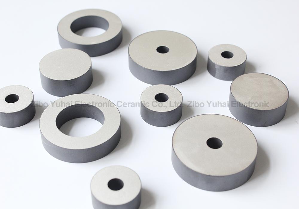
Lead Free Piezo Rings
Barium titanate lead-free piezoelectric
ceramics are important basic materials for the development of modern science
and technology, which was widely used in the manufacture of ultrasonic
transducers, underwater acoustic transducers, electroacoustic transducers,
ceramic filters, ceramic transformers, ceramic frequency discriminators, high
voltage generators, infrared detectors, surface acoustic wave devices,
electro-optic devices, ignition and detonation devices, and piezoelectric
gyroscope and so on.
Application: military, ocean, fishery, scientific research,
mine detection, daily life and other fields.

Piezoelectric Ring,Lead Free Piezoelectric Ring,Piezo Electric Ring,Lead Free Piezo Rings
Zibo Yuhai Electronic Ceramic Co., Ltd. , https://www.yhpiezo.com
