Jiang Yu, Zhang Yuxi, Ren Yanping, Pan Ruiyun, China Shipbuilding Industry Corporation
Keywords: VPX standard; FPGA; serial transmission
0 Preface
With the increasing demand for radar processing on processing speed, bus bandwidth, data processing and work environment, traditional radar signal processing systems have been unable to meet the actual requirements for technical development and model development. The VPX-based signal processing platform has powerful signal processing and data processing capabilities, as well as I/O capabilities and high-performance network switching capabilities. Because of this, the VPX standard represents the development trend and direction of a new generation of integrated information processing platform systems.
1 Introduction to VPX Standard
VPX is a new-generation bus standard based on high-speed serial buses. The original purpose of this standard is to protect the VME bus users, inherit and continue the VME bus. However, subsequent standard makers found that a small amount of repair work could not meet the demand, and thus thoroughly reformed many specifications. The VPX bus standard has the following outstanding advantages and advancements:
(1) Strong I/O capability and high-performance network switching capability to support higher backplane bandwidth, providing sufficient bandwidth and processing power for radar signal processing. The VPX standard defines a new 7-row high-speed I/O connector up to 6.25 Gb/s that fully supports the current high-speed serial interconnect standards. These standards include SRIO, PCIE, RocketIO, SATA, Gbit Ethemet and 10Gbit Ethemet. At the same time, the number of user-definable I/O pins has been greatly increased, providing sufficient space for future upgrades.
(2) The VPX standard defines the VPX card's external dimensions, the backplane's topological structure, the socket definition when supporting various serial standard protocols, the definition of the power socket, and the monitoring bus definition. This lays a solid foundation for the generalization of radar signal processing and data processing platforms.
(3) VPX standard is specially formulated for key high-performance systems. Its excellent thermal performance and highly reliable connectors give the system superior stability. At the same time, it has a strong and compact structure, good magnetic compatibility, and enhanced circuit boards and ultra-high power. Design and other features. Tests have shown that the VPX standard can meet the needs of military and aerospace and other harsh environments.
2 VPX system structure
The hardware system adopts the VPX architecture design. Each function is distributed on different VPX processing boards, and the data is interconnected through the backplane interconnection or the switching board. The main function boards include signal processing boards, switch boards, acquisition and storage boards, and backplanes. Signal processing and data processing board adopts general design (high-performance FPGA and dual-core CPU combined architecture), used for signal processing, detection, data processing and other functions, including DBF board, multi-block signal processing board, and host board.
The VPX chassis adopts a 7U ruggedized chassis and the power supplies are designed with dual redundant power supplies. There are a total of 10 VPX board slots (including 1 main board, 1 switch board, and 8 user-definable VPX boards). Interval 2.54cm. The VPX board is installed with positioning pins and guide rails. All boards are installed inside the VPX chassis.
3 system function
The system implements narrowband active radar signal processing functions. Radar signal bandwidth 5 MHz. The DBF board receives the quadrature baseband signals (20 MBps per unit) of each antenna element through multiple optical fibers, and transmits I and Q data of 8 antenna elements per optical fiber. The fiber data rate is 1.6 Gbps. Multiple quadrature baseband signals are amplitude-phase corrected and DBF beamformed on a DBF board to form multiple beam I and Q signals. The beamforming results are sent to the multi-block signal processing board through the high-speed differential serial line of the backplane. The number of signal processing boards required is determined by the number of beams formed by the DBF. Signal processing includes pulse pressure in the time domain, co-frequency interference (anti-asynchronous), moving target processing (MTI+MTD), modulus, logarithmic and constant false alarm. Signal processing block diagram shown in Figure 1.
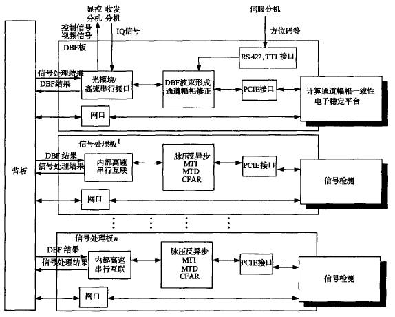
Figure 1 signal processing function block diagram
The moving target processing in signal processing adopts a pair of FIR filter bank elimination methods. The combined frequency response curve is shown in Figure 2.

Figure 2 One-time cancellation + FIR filter frequency response
Using the above moving target processing consumes a large amount of FPGA resources. In this system, each signal processing board has the ability to process five beams. The system has verified that 20 beams are formed at the same time after DBF, and four signal processing boards are used. All data exchange between boards adopts high-speed serial interconnection and the transmission rate is 1.6 Gbps. If the radar system needs to handle more beams, it only needs to increase the number of signal processing boards.
It can be seen that the signal processing platform using the VPX standard architecture can completely realize all the functions of the traditional active radar signal processing, and the system structure is more compact and reliable, the data interaction is more stable and efficient, and at the same time it has strong versatility and scalability.
4 FPGA programming points
This system uses simultaneous multi-wave speed operation and requires multiple signal processing boards to complete. This just reflects the superiority of the scalability of the VPX architecture board, and brings certain challenges to the data transmission and synchronization between the board and the board. The following points are summarized from the process of writing and debugging the program.
4.1 Estimation of FPGA Resources
The VPX standard architecture provides good versatility and extensibility for the system. Correctly estimating the FPGA resources before writing the program will provide a convenient system design.
Estimating the resource usage of the FPGA is aimed at determining the number of VPX integrated processing boards required for the entire system, and the upper limit of the number of VPX boards that can be used is determined by the data exchange format between the boards and the board and the topology of the backplane.
It is relatively easy to estimate the use of BLOCKRAM and multipliers within the FPGA. The estimated value is also relatively accurate. However, it is difficult to estimate the logics of the FPGA before writing the program. In the design, this system has experienced the need to increase the number of signal processing boards due to the lack of estimation of the logic resources, thus causing the program structure to change and the code to be modified in large quantities. The estimation of logical resources proposes the use of the “Expert Judgment Methodâ€, which means that a number of engineers with rich design experience give the logical resources required by the program and find their average values.
4.2 Serial Transmission Protocol and Transmission Rate Selection
The signal transmission between the VPX integrated processing boards uses the FPGA's internal GTX module for high-speed serial transmission. For XILINX's FPGA chip, serial transmission usually uses the aurora protocol or the custom Rocket-IO protocol. In this design, all the serial transmissions use the custom Rocket-IO protocol. This is mainly because the protocol is not encapsulated by the user, and the timing of the transmission can be accurately grasped so that the subsequent signal processing process is easy to operate. The aurora protocol is equivalent to a layer of user encapsulation based on the Rocket-IO protocol. Although the Rocket-IO complex control structure is converted into a simple user interface, it has simple and practical channel binding functions and efficient error correction functions. However, because the aurora protocol further encapsulates the original transmission, the timing of receiving is not so easy to control, and the user decides to select a custom Rocket-IO protocol.
When using serial transmission, the binding between channels is more important. For the binding of multiple optical fiber data with coherent transmission clocks, the channel binding function provided by the Rocket-IO core can be used. However, in most cases, the data is sent by different boards, and their sending clocks do not match. This can not directly use the IP core's own binding function, you need to use asynchronous FIFO as a flexible buffer to write a binding program, so that multiple serial data synchronization.
For the selection of the transmission rate between the board and the board, it is recommended to select a lower transmission data rate under the premise of satisfying the amount of data to be transmitted. This reduces the risk of bit errors in data transmission. In the debugging process of the system, a higher transmission rate was selected at the beginning, and it was found that bit errors occur frequently, and eventually the transmission rate is reduced to half of the original rate and the error disappears.
4.3 Cross Clock Domain Processing
The use of the VPX standard for signal processing inevitably involves the problem of processing across the clock domain. There may be multiple clock domains in the system at the same time. It is particularly important to plan the processing method across the clock domain before writing the program. For cross-clock domain processing methods, it is recommended that all received non-local clock domain data be first converted to the local clock domain, and then processed in the local clock domain. For parallel data, the asynchronous FIFO is used to convert to the local clock domain; for a signal with only 1 bit, a shot can be made directly in the process in the local clock domain. It should be noted that this signal must be held for more than 1 clock cycle, otherwise it may be lost.
4.4 Reset signal
All kinds of reset signals in the system should be given enough attention, especially when the system is complex and the reset signals are related to each other, the errors caused by incorrect reset settings are often not easy to modify. Firstly, synchronous reset is used as much as possible. A large number of synchronous designs provide many advantages for program debugging, making timing easier to meet and design more reliable. In the process of debugging the program, if there are some difficult to understand, no clue to the error, you can consider from the clock signal processing and reset signal settings. In this design, the improper handling of external memory Qdrsram, Rocket-IO core, FIR filter core reset will make the debugging process difficult.
4.5 Programming and Writing
Correct and efficient programming and writing provide great convenience for subsequent compiling, debugging, and addition and subtraction functions. The following summarizes several key points:
(1) The program must be written in a modular manner, which brings convenience to testing and finding errors.
(2) The preparation of the program should take into account the need for subsequent addition and subtraction functions. For example, in this design, if the signal processing function is added on the basis of the original requirements, each signal processing board will inevitably be able to process fewer beams. This requires the entire signal processing program to be modified. If this is taken into account in advance, each beam function is modularized so that even if the number of beams processed is increased or decreased, the procedure can be quickly modified. Need to add a comment to the more complex program structure, otherwise make the program readability reduced.
(3) Reasonable latching, clever use of flowing water structure. In the case of complex system functions and limited FPGA resources, it is necessary to ensure the implementation of functions and to reduce the use of logic resources. Correct programming methods can save a lot of logic resources. In the sliding and flowing signal processing process, if you can skillfully use the rules of the data loop to deal with, rather than simply use the register latch after processing, you can greatly reduce the writing space and save lots of lut resources. The latching of data is indispensable. Repeated latching is not only a waste of logic resources, which complicates subsequent compile times, but also fails to improve the FPGA processing speed.
(4) Make full use of the limited number of hard core resources inside the FPGA. FPGA internal hard-core resources (such as DCM, serial-to-parallel conversion, multipliers, etc.) are highly efficient, reliable, and do not occupy logic resources. Reasonable use of their characteristics can increase engineering reliability and reduce the use of logical resources. For example, it is necessary to complete clock phase-shifting or frequency division before phase shift processing. You can use two DCM cascade operations, or you can use PLL and DCM cascade operations; if you choose the latter, you save one DCM and the PLL has Smaller clock jitter, better results.
(5) Appropriate timing constraints. When the utilization of FPGA resources is high, proper timing constraints are very helpful for proper layout and routing. Excessive timing constraints can lead to unpredictable errors, too tight constraints, increased cabling time, and the possibility of wiring failures. The timing constraints can be increased (usually 5% to 10%) on the basis of the actual operating frequency, which makes the project more reliable. If you encounter the compile time sequence can not be fully satisfied, you must first view the timing report, modify the critical path does not meet the timing; if you can not meet, you can modify the ISE integrated, layout and wiring properties, that is, change the optimization strategy for speed, copy the register to open Etc.; if it is still not satisfied, it can only be operated manually.
5 Design experience
In the process of designing an active radar signal processing system using the VPX architecture, a deeper understanding of the flexibility and extensibility of the VPX architecture has been achieved:
(1) If an accurate estimate of board resources cannot be made before the design, only a few VPX board slots need to be reserved. Once there is insufficient resources, the card can be solved by adding boards.
(2) The signal transmission between the board and the board adopts the high-speed serial bus, which avoids the defects such as insufficient bandwidth and high bit error rate caused by parallel transmission in the past;
(3) The point-to-point high-speed serial interconnection provided by the VPX architecture provides enough bandwidth for signal processing. For radar systems that need to form multiple beams at the same time, the VPX architecture has obvious advantages;
(4) In terms of generality, the VPX architecture hardware platform has many processing capabilities and various bandwidths required by the radar system, which can meet the current needs of a variety of radar systems for signal processing and data processing, and avoids the repeated design of hardware. For radar systems with similar algorithms, only a small amount of software program modification is required to meet the requirements, which greatly saves design costs.
6 Conclusion
According to the demand analysis of radar system and the development trend of radar signal data processing technology, modern radar signal data processing platform will present a general platform design based on high-performance FPGA-based signal preprocessing plus multi-core PowerPC or multi-core CPU-based signal processing mode. It has the characteristics of signal processing and data processing compatibility, real-time operating system, and reconfigurable system architecture based on high-speed serial data exchange. The general signal processing and data processing platform based on the VPX standard well caters to this kind of development trend, making the VPX standard the best choice for military new generation standard buses. The system uses the characteristics of the VPX architecture rationally, realizes more complex active radar signal processing functions, verifies the feasibility of active radar signal processing based on VPX standards, and accumulates certain experience for subsequent active radar signal processing using VPX standards. .
Ceiling Type Plasma Air Sterilizer
Plasma Purifier,Hospital Uv Sterilizer,Plasma Air Sterilizer,Plasma Sterilization Equipment
Dongguan V1 Environmental Technology Co., Ltd. , https://www.v1airpurifier.com