High-precision time reference has become one of the basic guarantee platforms in the fields of communication, power and industrial control. The time system equipment usually uses a crystal oscillator as the frequency standard, but both of them have poor long-term stability due to crystal aging and temperature changes. With the development and application of GPS technology, GPS is used as an excellent feature of precise time source to synchronize local clock information. However, in practice, the 1pps signal provided by GPS is often interfered with, such as magnetic field interference, multipath error, etc., causing misinterpretation of the interference signal as a normal 1pps signal or GPS signal tracking loss, resulting in excessive error in the measurement and control system. Accuracy and stability are difficult to guarantee. Therefore, the 1pps signal cannot be directly used as a precise synchronization signal from the GPS receiver board, and must be processed by technology to maintain high precision and continuous stability. At present, the discrete documents or single-chip microcomputers are often used as the main controller for the above problems, and it is necessary to add a peripheral time interval measurement or equalization circuit, which is not suitable for the occasion of high voltage control crystal frequency.
In this paper, the 1pps second pulse signal provided by GPS is used to solve the above problem. On the basis of FPGA (fieldprogrammablegatearray), the method of interference second pulse signal elimination and deviation frequency average operation is used to reduce the peripheral circuit and reduce the randomness of the GPS clock signal. The interference error eliminates the accumulated error of the local crystal clock signal, thereby controlling the output frequency of the local voltage controlled crystal oscillator and improving the long-term stability of the crystal oscillator.
1. Frequency control system structure and working principleThe block diagram of the overall structure of the FPGA frequency control system is shown in Figure 1. The system input is the 1pps second pulse signal generated by the GPS receiver when tracking the satellite, the logic level output, the high level duration is 1.01±0.01ms, and the rising edge of the high level is used as the reference time for the output of the second pulse signal [9 -10]. The digital control circuit is the FPGA control circuit. The main control chip is EP1C6--144TQFP. It can be repeatedly programmed by software, modify the circuit scheme, and has fewer peripheral hardware circuits and high reliability. The circuit will measure the phase difference between the synchronous second pulse and the 1 pps second pulse generated by the local voltage controlled crystal oscillator, and obtain the relative frequency difference required for the synchronous signal by using the interference second pulse signal cancellation and the deviation frequency average operation. The D/A converter converts the relative frequency difference into an analog control voltage, and feeds back to the control end of the local constant temperature voltage controlled crystal oscillator to adjust the frequency signal of the high stable crystal oscillator, and reduces the synchronization difference with the 1 pps second pulse, thereby improving the high frequency accuracy of the oscillator. Degree and long-term stability, the taming function of the digital synchronous clock.
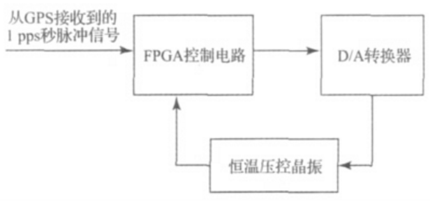
Figure 1 Overall structure of the FPGA frequency control system
2, system function designSystem function design mainly includes hardware design and software design 2, as shown in Figure 2. The software implementation part is: VHDL programming language to realize the taming function of GPS signal to crystal oscillator, including how to eliminate GPS interference signal, realize GPS synchronous clock method, continue to tame the crystal frequency after losing GPS signal, and output local synchronization Second clock signal. The hardware implementation part is: the D/A converter provides the converted analog control voltage, and the constant temperature voltage controlled crystal oscillator calibrates the frequency according to the analog voltage and feeds back to the FPGA processor.
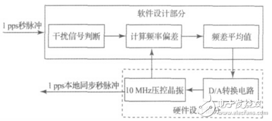
Figure 2 system function design
2.1, interference signal judgment and eliminationThe 1pps second pulse signal is output in the form of a square wave. The high level indicates that there is a second pulse output. The high level pulse width is not a constant value. The duration is about 1ms and there is an error of 0.01ms, which results in a high period of 1pps signal. The crystal count values ​​are not equal. In addition, due to interference, the received 1pps signal has an interference pulse signal. If the rising edge of the interference pulse is counted as the rising edge of the 1pps signal, the counting result is inevitably inaccurate, and the measured crystal frequency value deviates too much from the actual value. The software is required to determine the interference signal and process it.
The high-level duration of the interference pulse in the digital circuit is mostly microsecond, and there is rarely more than 1pps second pulse signal high-level duration. Therefore, the second pulse high-level duration is used as the basis for judging the local voltage-controlled crystal oscillator. Count to achieve timing. The nominal frequency of the crystal oscillator is 10 MHz, and the theoretical value of the count value of 2 ms is 20000. On the premise that the crystal high-frequency pulse output occurs clk'eventandclk='1', the 1pps signal event sclk'eventandsclk='1' is started to count, and the counter value is saved by the register counter4, such as a pulse exceeding 2ms high level. The signal is a normal 1 pps signal. If it is less than 2 ms, it is considered as an interference signal, and the register counter4 count value returns to the count value before the rising edge of the signal pulse.
2.2, frequency deviation value calculationIn order to calibrate the crystal output signal frequency, it is necessary to calculate the frequency deviation value, calculate the corresponding adjustment value, change the analog voltage through the D/A converter, and feed back to the constant temperature voltage control crystal oscillator to achieve the purpose of adjustment. The quadratic regression model can be used to analyze the frequency deviation of the output crystal second clock and the GPS second clock.
Due to the short-term stability of the local constant temperature voltage controlled crystal oscillator, less than 1 & TImes; 10-10 / s, the random error of the crystal oscillator second pulse can be ignored, only the frequency deviation and linear drift error caused by the cumulative error are considered, and the crystal frequency division second time series The time error e(x) of the xth second clock is:
e(x)=a+bx+cx^2(1)
Where: a is the initial error of the second time series, b is the error coefficient of the frequency deviation, and c is the error coefficient of the linear drift of the frequency.
Through the quadratic regression analysis, the crystal error estimate of equation (1) is obeyed by a normal distribution:
^e(x)=^a+^bx+^cx2~N(a+bx+cx2,D(^e))(2)
According to the regression analysis, it is found that when x = n, the variance of the time error of the second clock has a maximum value Dmax. By analyzing the relationship between the maximum variance Dmax of the above formula and the number n of regression analysis samples, the larger the sample number n, the smaller the maximum variance Dmax, that is, the smaller the deviation between the crystal frequency division second pulse and the GPS second clock. However, the number of samples n cannot be infinitely large, and is limited by the hardware and software resources of the FPGA. Generally speaking, when n≥3, the time deviation of the adjusted crystal frequency division second pulse is smaller than the deviation of the GPS second clock, which can meet the requirement.
The above method needs to accumulate the crystal oscillator count value within 1 s, and requires a 24-bit register to store the count value, which requires too much processing speed of the chip operation, and occupies more FPGA resources, affecting the control speed. On this basis, this paper adopts the method of deviation frequency averaging operation. That is, the deviation value of the crystal oscillator frequency-divided second pulse and the GPS second clock is obtained every s, and every 3 samples time is used as the control cycle period, and the total deviation value in 3s accumulation is Z=Z1+Z2+Z3, and the average deviation of the cycle period is obtained. The value Z0=Z/3, in the next cycle sample period, feedback to the crystal oscillator every second, adjust the crystal oscillator output frequency.
The specific method of the crystal frequency division second pulse and the GPS second clock deviation value is as follows: the counter value of the crystal oscillator is stored in the register counter1, and the theoretical count value is 1 & TImes; 107 crystal oscillation pulses. The register counter2 is the second clock counter. When it is judged that the 1pps signal is a non-interfering signal, the register counter2 is incremented by one. The deviation of the normal second pulse frequency is within the range of ±128. If the deviation exceeds the range, it is an out-of-tolerance signal and is not processed. Therefore, the lower 8 bits of the register counter1 are used as the register counter3 of the error frequency. When the counter2 value reaches the loop control sample number 3, the average deviation frequency is calculated, and the result is stored in the register-counter7 output.
The simulation waveform of the scheme is shown in Figure 3. Because the theoretical count value is large, the actual program operation time is too long, and the result is difficult to clearly observe. The number of crystal oscillator pulses in one second pulse time is reduced to 15 crystal oscillator pulses. Data reduction does not affect the verification of the scheme. It can be seen that in the one control loop period in which the counter2 register counts up to 3 seconds, the frequency average error of the lower 8 bits is 15, and the remainder obtained by the counter7 register is also 0001111. The results show that the scheme can accurately obtain the frequency deviation value.
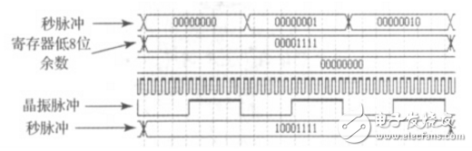
Figure 3 scheme simulation waveform
Wireless Charging Coils,10W Wireless Charging Coil,Wireless Charging Coil For Cell Phone,Car Wireless Charging Coils
Shenzhen Sichuangge Magneto-electric Co. , Ltd , https://www.scginductor.com