With the popularization of mobile devices such as notebook computers, mobile phones, and PDAs, the development of integrated circuits for various battery power sources has become more and more active, and high-performance, low-cost, ultra-small package products are accelerating commercialization. LDO (Low Dropout) type linear regulators have been widely used in portable electronic products due to their simple structure, low cost, low noise and small size.
In portable electronics, higher power efficiency means longer battery life, while linear regulator efficiency = output voltage & TImes; output current / input voltage & TImes; input current & TImes; 100%, therefore, the input and output voltage difference The lower the quiescent current (the difference between the input current and the output current), the higher the efficiency of the linear regulator.
The low-dropout linear regulator designed in this paper has an output voltage of 2.5V or an adjustable output. When the load is 1mA, the minimum input-output differential voltage is 0.4mV. When the load is 300mA, the voltage difference is 120mV. The power supply voltage works. The range is 2.5 to 6V.
Circuit structure and working principle
The circuit structure of the low dropout linear regulator is shown in Figure 1. The circuit consists of a regulation tube, a bandgap reference voltage, an error amplifier, a fast start, an overcurrent limit, an overheat protection, a fault detection, and a sampling resistor network. With enable, output adjustable and other functions. Adjusting the tube as a load device with differential pressure, to meet the requirements of this design, it should be considered for its choice: first compare the triode and MOS tube, because the triode is a flow control device, and the MOS tube is a voltage control device, in comparison MOS The quiescent current of the tube structure is lower. Secondly, the NMOS transistor needs a driving signal higher than the output voltage, and the PMOS transistor does not have such a requirement, and it is difficult to generate a high driving voltage especially at a low input voltage. Therefore, this paper uses a PMOS tube as the adjustment tube.
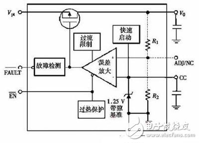
Figure 1 Low-dropout linear regulator circuit structure
The working principle of the circuit is: during the power-on process of the circuit, there is a 500μA current source in the fast-start circuit to charge the bypass capacitor C of the CC terminal, so that the circuit is powered on as soon as possible, and the non-inverting terminal of the error op amp passes the sampling resistor R1. R2 samples the output voltage V0, compares it with Vref, and then outputs an amplified signal to control and adjust the gate voltage of the PMOS transistor to keep the output voltage V0 stable, that is:
When the circuit has overcurrent or overheat condition during the working process, the overcurrent limit and the overheat protection circuit will respond quickly, the conduction state of the adjustment tube will be weakened and turned off, the protection circuit will not be damaged, and the fault detection circuit will produce a low Level signal. When the enable terminal is high, the circuit works normally; when the enable terminal is low, the reference circuit and the adjustment PMOS transistor are turned off, and the circuit is in a waiting state.
Key feature analysis and design considerations
1. Leakage voltage (VDO) and quiescent current (Iq)
Leakage voltage is defined as the minimum input-to-output voltage difference that maintains the regulator's normal operation. It is an important factor in reflecting the adjustment capability of the regulator. For a circuit using a PMOS transistor as the regulation transistor, the leakage voltage is determined by the on-resistance (Ron) and the load current (Io), namely: VDO = Io & TImes; Ron. The quiescent current of the low-dropout linear regulator is the input current and the output current. The difference is: Iq = Ii - Io. The quiescent current consists of the bias current and the gate drive current of the regulator. For a PMOS pass transistor, the gate is driven by a voltage and generates almost no power. When the regulator is carrying a small load or no load, the leakage voltage is extremely low, and the quiescent current is equal to the total bias current when the regulator is operating. When designing, pay attention to make the on-resistance and leakage current of the PMOS regulator tube as small as possible, and each module circuit can work normally under a small current state.
2. Power consumption (Pw) and efficiency (η)
The power consumption of a low dropout linear regulator is the difference between the input energy and the output energy, namely:
PW = VI II - VO IO = ( VI - VO) IO + VI Iq
In the above formula, the former is the power consumption generated by the regulation tube, and the latter is the quiescent current power consumption. The regulator efficiency can be expressed as follows:
η= IO VO / ( IO + Iq ) VI×100 %
The expressions for power consumption and efficiency fully demonstrate that for low dropout linear regulators, low leakage voltage and low quiescent current mean low power consumption and high efficiency.
3. Load adjustment capability and voltage adjustment capability
Load regulation capability refers to the ability of the output voltage to maintain a certain value when the output current changes. It is defined as: ΔVO / ΔIO, which characterizes the load change and the regulator's ability to maintain the output at a nominal value. The smaller the value, the better. . Voltage regulation capability refers to the ability of the output voltage to maintain a certain value when the input voltage changes, defined as: ΔVO / ΔVI, which characterizes the input voltage change and the regulator's ability to maintain the output at a nominal value. The better. The load adjustment capability and voltage adjustment capability of the circuit structure of Figure 1 are:
Where gm is the transconductance of the adjustment tube; Aod is the open-loop differential mode gain of the error amplifier; Rds is the equivalent resistance between the source and drain of the adjustment tube; RL is the load resistance; R1 and R2 are the sampling resistors. It can be seen from the above equation that the key to reducing ΔVO÷ΔIO and ΔVO÷ΔVI is to increase gm and Aod as much as possible.
4, transient response
The transient response is the dynamic characteristic of the regulator. It refers to the transient pulse phenomenon of the output voltage caused by the step change of the load current and the stable time of the output voltage recovery. The equivalent series resistance RESR of the output capacitor COUT and the output capacitor, and the bypass. The capacitance Cb is related, and the maximum transient voltage pulse value ΔVTR(MAX) is:
Where: IO(MAX) is the maximum load current in which the step change occurs; Δt1 is the response time of the regulator closed-loop, which is related to the closed-loop bandwidth of the regulator (0dB frequency point). Design applications should consider reducing the transient voltage pulse of the regulator, which increases the bandwidth of the regulator, increases the output and bypass capacitors, and reduces its equivalent resistance.
5, output accuracy
The output accuracy of the regulator is a combination of various factors at the output. It mainly includes the output change ΔVLR caused by the input voltage change, the output change ΔVLDR caused by the load change, the output change ΔVref caused by the reference drift, and the error amplifier. The output change ΔVamp caused by the offset, the output change ΔVres caused by the drift of the resistance of the sampling resistor, and the output change ΔVTC caused by the change in the operating temperature, the output accuracy ACC is given by:
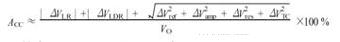
Among them, ΔVref, ΔVamp and ΔVres have a great influence on ACC, so the topology of the reference voltage source, error amplifier and sampling resistor network should be considered in the design.
Industrial Lighting Led Driver
IP65 or IP67 for waterproof, products applicable to Industrial and high bay light for outdoor, also pass the UL/FCC/TUV/RCM/CB/CE Certified. can do the dimming 0-10V/PWM/RX. With the short circuit, over temperature, over voltage protaction. Stable performance, can be used for a long time.Good water resistance, the use of safe and stable.
Parameter:
Input voltage: 100-277vac / 100-347V
output voltage: 25-40vdc / 27-42vdc / 35-45vdc / 50-70vdc / 12Vdc / 24vdc /36V/48V
current: 100mA-8000mA.
Power factor: >0.9
IP degree: IP65/ IP67
Dimming:0-10V / PWM / RX / DALI.
>=50000hours, 5 years warranty.

FAQ:
Question 1:Are you a factory or a trading company?
Answer: We are a factory.
Question 2: Payment term?
Answer: 30% TT deposit + 70% TT before shipment,50% TT deposit + 50% LC balance, Flexible payment
can be negotiated.
Question 3: What's the main business of Fahold?
Answer: Fahold focused on LED controllers and dimmers from 2010. We have 28 engineers who dedicated themselves to researching and developing LED controlling and dimming system.
Question 4: What Fahold will do if we have problems after receiving your products?
Answer: Our products have been strictly inspected before shipping. Once you receive the products you are not satisfied, please feel free to contact us in time, we will do our best to solve any of your problems with our good after-sale service.
Industrial Lighting Led Driver
Surge Protection Device,0-10V Dimming Led Driver,Led Grow Light Driver,Switching Power Supply
ShenZhen Fahold Electronic Limited , https://www.fahold.com