The 555 timer is a mid-scale integrated device that combines analog and digital functions. It is called 555, which is usually fabricated by bipolar (TTL) process. It is called 7555 by complementary metal oxide (CMOS) process. In addition to single timer, there is corresponding double timer 556/7556. 555 timer The wide supply voltage range is 4.5V~16V, the 7555 can operate from 3~18V, and the output drive current is about 200mA, so its output is compatible with TTL, CMOS or analog circuit levels. In 1972, the United States SigneTIcs developed the 555 timer to replace the medium-scale integrated circuit of the mechanical timer, named after the input design of three 5kΩ resistors.
First, the basic principle
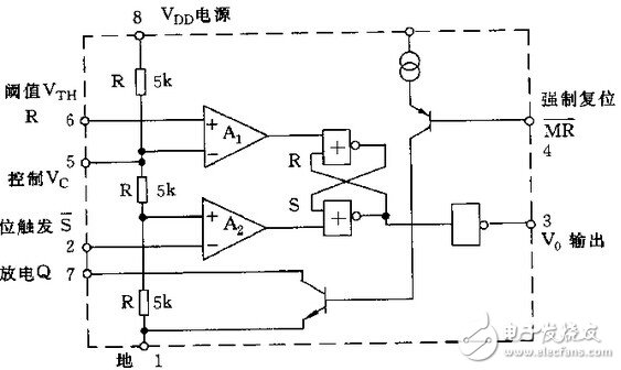
The working process of the 555 time base circuit is as follows: When the 2 pin, that is, the inverting input terminal of the comparator A2, is added with a trigger signal whose potential is lower than ?VDD, then VT9 and VT11 are turned on, and the VTl4 in the flip-flop is given. Provide a bias current, make VTl4 saturation conduction, its saturation voltage drop Vces clamps the base of VTl5 at a low level, makes VTl5 cut off, VTl7 is saturated, so that VTl8 is cut off, VTl9 is turned on, VT20 is fully saturated, VT21 cutoff . Therefore, the output 3 pin outputs a high level. At this time, regardless of the level of the 6-terminal (threshold voltage), due to the positive feedback of the 4.7kΩ resistor in the flip-flop (VTl4-VT17) (the base current of VTl5 is supplied through the resistor), The 3-pin output high state is maintained until the 6-pin appears above the VDD level. When the trigger signal disappears, that is, the potential of the inverting input terminal 2 of the comparator A2 is higher than ?VDD, then VT9 and VTll are turned off, and VTl4 is turned off due to no bias current. At this time, if the 6-pin has no trigger input, the Vces of the VTl7 is saturated. The voltage drop maintains the VTl3 cut-off through the 4.7kΩ resistor, so that the VTl7 saturation steady state does not change, so the output terminal 3 still maintains a high level. At the same time, the cutoff of VTl8 also cuts off VT6. When the trigger signal is applied to pin 6, and the potential is higher than ?VDD, then VTl, VT2, and VT3 are all turned on. At this time, if there is no external trigger signal on the 2 feet to turn off VT9 and VTl4, the collector current of VT3 is biased to VTl5, so that the stage is saturated, and VTl7 is turned off, and then VTl8 is turned on, VTl9, VT2. Both are off, VT21 is saturated, so the 3 pin outputs low level. When the trigger signal of the 6-pin disappears, that is, when the potential of the pin falls below VDD, VTl, VT2, and VT3 are all turned off, so that VTl5 cannot be biased. At this time, if there is no trigger signal on the 2 pin, VTl5 will get a bias current through the 4.7kΩ resistor, so that VTl5 maintains saturation conduction, and the steady state of VTl7 is cut off, so that the 3-pin output terminal is maintained at a low level. At the same time, the conduction of VTl8 makes the discharge stage VT6 saturate and conduct. Through the analysis of the above two states, it can be found that as long as the potential of the 2 pin is lower than ?VDD, when the trigger signal is added, the output pin 3 must be high; and when the potential of the 6 pin is higher than ?VDD When the trigger signal is added, and the potential of the 2 pin is higher than VDD, the output pin 3 has a low level output. 4 feet are the reset end. When a trigger signal is applied to the pin, that is, its potential is lower than the on-state saturation voltage drop of 0.3V, VT8 is turned on, and its emitter potential is lower than lV. Because D3 is connected, VTl7 is off state, VTl8, VT21 The saturation is turned on, and the output pin 3 is low. At this time, regardless of the potential of the 2nd and 6th feet, this state cannot be changed. Since the emitter of VT8 passes through the emitters of D3 and VTl7 to ground, the emitter potential of VT8 will not be higher than the 1.4V voltage under any circumstances. Therefore, when the potential of the reset terminal 4 is higher than 1.4V, the VT8 is in a reverse bias state and does not function, that is, the level of the output pin 3 at this time depends only on the potentials of the 2 pin and the 6 pin.
Buffet Warmer,Food Warmer,Stainless Steel Food Warmer,Unter Top Buffet Food Warmer
Shaoxing Haoda Electrical Appliance Co.,Ltd , https://www.zjhaoda.com