1 Introduction
With the development of science and technology, experimental measurements under extreme conditions have become an important means of further understanding of nature. These tests often measure some very weak physical quantities, such as weak magnetic, weak sound, weak light, weak vibration, etc. These weak signals are generally converted by a sensor to convert the weak signal to be measured into an electrical signal. In actual measurement, noise and interference cannot be avoided, which affects the sensitivity and accuracy of the measurement. For the purpose of studying the measurement of pA-level current, a micro-current measuring instrument with an accuracy of 0.5 is developed. The minimum range of measurement is 10 pA. For pA-level current measurement, the measuring circuit cannot directly capture the current signal, and I/U is required. Conversion. The converted voltage signal needs to be further amplified, otherwise it will be interfered by the DC signal of the op amp's offset voltage and bias current. The problem is that while the signal to be tested is amplified and captured, the impurity signals such as power frequency interference, noise, and circuit offset are also amplified at the same time, so it is necessary to design a relevant subsequent circuit to filter and remove. For power frequency interference, it can be shielded and filtered. The elimination of these DC impurity signals, such as circuit offset, is the core of this paper. It is to filter out these impurity DC signals by using modulation circuit and differential circuit.
2 micro current measurement method overview
2.1 Measurement method
Weak signal detection is to filter out the interference signal from the signal source, enhance/maximize the useful signal to be tested, improve the signal-to-noise ratio (SNR), and effectively suppress the noise is the difficulty and focus of the micro-current measurement. The proposed micro-current detection method and the development of micro-current measuring instrument are currently a hot spot in this field. As far as the detection method is concerned, there are mainly: sampling integration method, correlation detection method, noise analysis method, modulation and demodulation method, wavelet transform method, high impedance input method, photoelectric coupling method, integrated operational amplifier, computer program control, etc., but The sampling resistance method and the op amp feedback current method are commonly used methods for micro current measurement.
Noise interference is an effective suppressive interference signal. According to the type and characteristics of noise, there are two main sources: 1) inherent noise from the electronic system, including the bias current of the op amp, the offset voltage, and the heat generated by the electronic components. Thermal noise, pulsed noise generated by digital circuit interference, spike noise generated by switching circuits, etc.; 2) from outside the electronic system, such as power frequency interference, radio frequency noise, atmospheric noise, mechanical noise, etc. In the measurement, the processing of noise is extremely important. It is proposed that the key to the micro-current measurement is to suppress the circuit impurity DC signal and power frequency interference.
2.2 Development status of micro current measurement technology
With the technical advantages of sensitive current measuring instruments, Keithley has developed the 6482 dual-channel picoammeter/voltage source with a measurement resolution of up to 1 fA, 6 and a half, and a measurement range of 2 nA to 20 mA.
3 design theory
3.1 Micro current - voltage conversion principle
It can be known from the Thevenin's theorem that any two-end network can be regarded as an equivalent voltage source Us and the equivalent resistance Rs in series, that is, Rs=Us/Is. The measurement principle of the operational amplifier feedback current method is shown in Fig. 1.
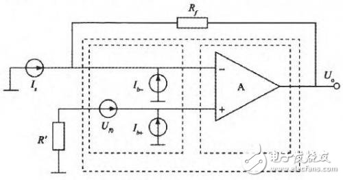
Figure 1 Principle of op amp feedback current measurement
In the figure: Rf is the feedback resistor; R' is the balance resistor; UI0 is the op amp offset voltage; Ib-, Ib+ is the op amp bias current; Is is the microcurrent to be tested; Uo is the output voltage.
The ideal circuit output is Uo= - IsRf. Since the op amp has offset voltage and bias current, the actual circuit output is:
U'o= - IsRf+UI0+Ib+R'+Ib-Rf (1)
The voltage output error is:
â–³Uo=UI0+Ib+R'+Ib-Rf (2)
3.2 differential, modulation circuit principle
A measurement method that uses differential and modulation circuits to filter out DC impurity signals in the circuit is proposed to completely eliminate the interference generated by the circuit itself in the micro current measurement process. Differential and modulation means that the modulation switch is controlled by the central processing unit to modulate the micro current. By using a modulation circuit and a differential circuit to filter out the DC signals of these impurities, a micro pressure signal proportional to the signal to be measured is obtained. The principle of differential and modulation circuit is shown in Figure 2.
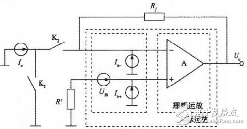
Figure 2 weak current differential, modulation preamplifier model
When K1 is disconnected, K2 is closed, ie output:
U01= IsRf+UI0+Ib+R'+Ib-Rf (3)
When K1 is closed, K2 is disconnected, ie output:
U02= UI0+Ib+R'+Ib-Rf (4)
By subtracting equation (4) from equation (3), the systematic error can be eliminated, namely:
Uo=U01- U02= IsRf(5)
It is known from equation (5) that the DC impurity signal is cancelled, and it can be seen that Uo is proportional to Is. However, the Uo signal is extremely weak, and Uo needs to be amplified by layers and then differentiated. Let the total magnification be K, then the output is: Uo=KIsRf; the measured microcurrent is:
Is=Uo/(KRf) (6)
The measurement results are sent to the central processor of the instrument and finally displayed through the display circuit.
Babbitt Wire is with tin as the base, the product is added with certain amount of antimony, copper
or other improved elements.
Sn Sb7Cu3 Babbit metal is suitable for metal spraying on the end face of metalized ï¬lm capacitor. With strong adhesive force, good weldability and low loss angle, it is an ideal metal spraying material for laminated capacitor.
Other trade marks are suitable to use CMT, TIG and MIG technology to manufacture sliding bearing bush material layer. It is of high bonding strength with substrate, with material utilization rate of 70~80%. It has small amount of ingredient segregation without any loose or slag inclusion. The internal control standard of the alloy composition is prevailing over GB/T8740-2013. Babbi1 metal added with improved elements can substantially enhance the service life.
Snsbcu Babbitt Wire,Overlaying Materials,Thermal Spray Babbitt Wire,Babbitt Wire
Shaoxing Tianlong Tin Materials Co.,Ltd. , https://www.tianlongspray.com