Abstract: The charger for the car battery of electric vehicles is discussed. According to SAE J1773, the design criteria of inductive coupler and different charging modes are given. A variety of alternative design schemes are given, and the most suitable circuit topology schemes are given for different charging modes and charging levels.
This article refers to the address: http://
Keywords: electric vehicle; charger; topology selection
0 Preface
As early as the early 20th century, electric drive systems were used in car drive systems in Europe and the United States. Electric cars at that time replaced the old carriages and bicycles as the main means of transportation. The advantages of electric vehicles, such as comfort, cleanness, noise-free, and low pollution, once made people think that this would be a huge innovation in transportation. However, due to the troubles of key technologies such as batteries at the time and the development of fuel vehicles, the development of electric vehicles has been limited for 100 years.
With the development of modern high-tech and the increasingly prominent problems of the world's environment and energy, electric drive vehicles have become a hot spot in the research, development and use of the automotive industry. Since the 1980s, countries around the world have set off a climax of large-scale development of electric vehicles. But the marketization of electric vehicles has been plagued by some key technologies. Among them, one of the more prominent problems is to ensure the safe, efficient, user-friendly, firm and cost-effective charging technology of electric vehicle battery packs [1][2].
1 charging technology
Electric vehicle battery charging is one of the key technologies that must be solved before electric vehicles are put on the market. Electric vehicle battery charging generally uses two basic methods: contact charging and inductive coupling charging.
1.1 Contact charging
The contact charging method uses a conventional contactor, and the user connects the charging source connector to the car. A typical example is shown in Figure 1. The drawback of this approach is that the conductor is exposed outside and is not safe. Moreover, due to multiple insertion and removal operations, mechanical wear is caused, resulting in loose contact and inability to efficiently transfer electrical energy.
Figure 1 Contact charging diagram
1.2 Inductively coupled charging
Inductively coupled charging mode, that is, no direct electrical contact is adopted between the charging source and the vehicle receiving device, and a combination of separated high-frequency transformers is used to transmit energy without contact through inductive coupling. The inductively coupled charging method can solve the defect of the contact charging method [3][4].
Figure 2 shows a simplified power flow diagram for an inductively coupled charging system for an electric vehicle. In the figure, after inputting the grid AC power, it is rectified, passed through the high-Frequency Inverter link, transmitted through the inductive coupler through the cable, transmitted to the input end of the electric vehicle, and then rectified and filtered to charge the electric vehicle battery.
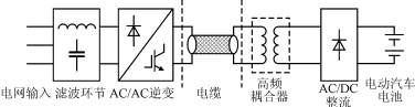
Figure 2 EV inductively coupled charging system simplified power flow diagram
The inductively coupled charging method can be further designed as a fully automatic charging method without human intervention. That is, the magnetic coupling device of the inductive coupler is separated by a larger distance between the primary and secondary sides, and the charging source is installed at a fixed location. Once the car is parked at the fixed area, the energy of the charging source can be received without contact. Inductive charging is realized, so that automatic charging is realized without the intervention of the vehicle user or the charging station staff.
2 Inductively Coupled Charging Standard—SAE J-1773
In order to realize the marketization of electric vehicles, the American Automobile Engineering Association has established corresponding standards according to system requirements. Among them, for the charger of the electric vehicle, two charging standards of SAE J-1772 and SAE J-1773 are formulated, which correspond to the contact charging method and the inductive coupling charging method respectively. Manufacturers of electric vehicle charging systems must meet these standards in the design and development of electric vehicle chargers.
The SAE J-1773 standard specifies the minimum actual size and electrical performance requirements for inductive charging couplers for electric vehicles in the United States.
The charging coupler consists of two parts: a coupler and a car socket. The combination is equivalent to a transformer that operates between the primary and secondary sides operating at frequencies between 80 and 300 kHz.
For inductively coupled electric vehicle charging, SAEJ-1773 recommends three charging methods, as shown in Table 1. For different charging methods, the design of the charger will be different accordingly. Among them, the most common way is the household charging mode, the charger power is 6.6kW, and the higher power level charger is generally used in charging stations and the like.
Table 1 Three charging modes recommended by SAEJ-1773
| Charging mode | charging method | Power level | Grid input |
|---|---|---|---|
| Mode 1 | Emergency charging | 1.5kW | AC120V, 15A single phase |
| Mode 2 | Household charging | 6.6kW | AC230V, 40A single phase |
| Mode 3 | Charging station charging | 25 to 160 kW | AC208~600V three phase |
According to the SAE J-1773 standard, the inductive coupler can be represented by the equivalent circuit model shown in FIG. The corresponding component values ​​are listed in Table 2.
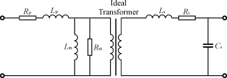
Figure 3 Inductive Coupler Equivalent Circuit Model
Table 2 Inductive Coupler Equivalent Circuit Model Component Values ​​for Charging
|   | f min (100kHz) | f max (350kHz) |
|---|---|---|
| R pmax /mΩ | 20 | 40 |
| L p ±10%/μH | 0.8 | 0.5 |
| R smax /kΩ | 1.6 | 1.3 |
| L s ±10%/μH | 45 | 55 |
| R mmin /mΩ | 20 | 40 |
| L m ±10%/μΗ | 0.8 | 0.5 |
| C s /μF | 0.02 | 0.02 |
| Debbie | 4:4 | 4:4 |
| Every åŒ voltage / V | 100 | 100 |
| Coupling efficiency /% | ≮99.5 | ≮99.5 |
| Insulation resistance / MΩ | 100 | 100 |
| Maximum charging current / A | 400 | 400 |
| Maximum charging voltage / V | 474 | 474 |
The original secondary side of the transformer is separated and has a large air gap. It belongs to loosely coupled magnetic parts, and the magnetizing inductance is relatively small. When designing the converter, the influence of this small magnetizing inductance on the circuit design must be fully considered [5].
Power transmission cables must still be considered in the design. Although this item is not included in the SAE J-1773 standard, the volume, weight, and equivalent circuit of the power transmission cable must be considered in the actual design. Since the size of the transmission cable is mainly related to the level of the transmission current, reducing the charging current can correspondingly reduce the cable size. In order to minimize cable power loss, coaxial cables can be used to optimize at the operating frequency range. In addition, the cable introduces additional impedance, increasing the equivalent leakage inductance of the transformer, which must be considered in the design of the power stage. For a 5 m long coaxial cable, the typical resistance and inductance values ​​are: R cable = 30 mΩ; L cable = 0.5 to 1 μH.
3 Requirements for inductively coupled charge converters
According to the inductive coupler equivalent circuit given by the SAE J-1773 standard, the characteristics of the connecting cable and the battery load, it can be concluded that the inductively coupled charging converter should meet the following design criteria.
3.1 Current source high frequency chain
The secondary side filter circuit of the inductively coupled charging converter is mounted on the electric vehicle. Therefore, the capacitive filtering circuit used in the filtering step will simplify the vehicle circuit, thereby reducing the weight of the entire electric vehicle. For capacitive filtering, the converter should be characterized by high frequency current sources. In addition, this current source type circuit is relatively less sensitive to converter operating frequency variations and power level variations, and thus it is easier to simultaneously consider three charging modes for circuit design. Moreover, the secondary side uses a capacitive filter circuit, and the secondary side diode does not need to use overvoltage clamping measures.
3.2 Soft switching of the main switching device
The high frequency of the inductively coupled charging converter can reduce the volumetric weight of the inductive coupler and the on-board filter component, and achieve miniaturization of the power supply system. However, as the frequency continues to increase, the converter with a hard switching mode will greatly increase the switching loss and reduce the efficiency of the converter. Therefore, in order to achieve higher frequency, higher power level charging, it is necessary to ensure soft switching of the main switching device and reduce switching loss.
3.3 Constant frequency or narrow frequency range of operation
Inductively coupled charging converters operate at constant frequency or narrow frequency variations to facilitate optimal design of magnetic components and filter capacitors. At the same time, it is necessary to avoid operating in the radio bandwidth and strictly control electromagnetic interference in this area. For frequency conversion work, light load corresponds to high frequency operation, and heavy load corresponds to low frequency operation, which is beneficial to the efficiency under different load conditions.
3.4 Wide load range operation
The inductively coupled charging converter should be able to operate safely over a wide load range, including the limits of open and short circuits. In addition, the converter should also be able to operate in trickle charge or equalization charging modes. In these modes, the converter should be able to guarantee higher efficiency.
3.5 Inductive coupler ratio
The ratio of the primary and secondary sides can make the primary current smaller, so that a thinner power transmission cable can be used, and the efficiency of the lower current rated power device is improved.
3.6 Input unit power factor
The inductively coupled charging converter operates at high frequencies and can cause harmonic pollution to the power grid. Inductive charging technology must be recognized by the public and widely used. Effective measures must be taken, such as power factor correction or reactive power compensation, to limit the total harmonics of the inductively coupled charging converter of the electric vehicle entering the grid. For the time being, the charging converter must meet the IEEE 519-1992 standard or similar standard. To meet these standards, the complexity of the input portion of the inductively coupled charging converter and the whole machine is increased, which increases the cost. Moreover, according to different charging level requirements, the inductively coupled charging converter can select a two-stage structure (the front stage is PFC + the latter stage is the charger circuit) or a single-stage circuit in which the PFC function and the charging function are integrated.
4 converter topology selection
According to the equivalent circuit component values ​​of the inductive coupler given in SAE J-1773, and the above design considerations, the converter topology suitable for three different charging modes is examined here.
As shown in FIG. 2, the vehicle-mounted part of the electric vehicle includes a jack portion of the inductive coupler and an AC/DC rectification and capacitive filter circuit. First, the rectifier circuit that directly connects the capacitor filter is investigated. Suitable rectification methods include half-wave rectification, center-tap full-wave rectification and full-bridge rectification. Among them, the half-wave rectification has low utilization rate of the transformer; the full-wave rectification requires two windings with the secondary side connected by the center tap, which increases the weight and volume of the on-board circuit; the full-bridge rectification has high utilization rate of the transformer, and is suitable for use in this. Kind of occasion.
Figure 4 shows a block diagram of the inductively coupled charging converter based on the above considerations. In the figure, the output rectification uses a full-bridge rectification circuit, the output filter uses capacitive filtering, and the input end uses a PFC circuit to limit the total harmonics entering the grid without exceeding the standard. Here, a separately designed PFC stage is used. At low power, the PFC can also be combined with the main charging converter as an integrated charging circuit with PFC function.
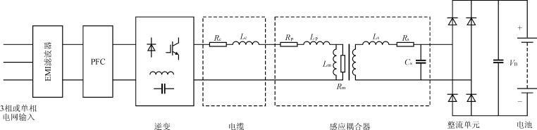
Figure 4 is a schematic block diagram of the inductively coupled charging converter
As mentioned earlier, one of the most important considerations in charger design is the reasonable selection of the inductive coupler ratio. In order to standardize the design, inductively coupled charging converters designed in three charging modes must be able to use the same electric vehicle socket. Factors limiting the number of turns on the secondary side of the charger's high frequency transformer include wide power range, electrical design constraints, and mechanical design constraints. A typical coupler design has a secondary side turns of 4 turns. For low charge levels, a 1:1 turn ratio is typically used, and for high charge levels, a 2:1 turns ratio is typically used.
For the energy storage capacity within 30 kW·h, the battery voltage of the electric vehicle varies from DC 200 to 450 V depending on the state of charge. The converter topology should be able to provide the required charging current within the range of this battery voltage variation.
4.1 Charging mode 1
This is an emergency charging mode for electric vehicles, which is slower to charge. Chargers designed in this mode are typically carried with electric vehicles and are used without a standard charger, which necessitates small size, light weight, and low cost. According to these requirements, a single-stage high power factor converter can be used to reduce the overall size, weight, and cost, and achieve higher overall machine efficiency. Figure 5 shows an alternative: an isolated Boost converter with two switching tubes [6]. The single-stage Boost stage circuit provides PFC functionality and regulates the output voltage when no auxiliary switches are used. When the input voltage is AC 120V, the input voltage peak value is 170V. Since the transformer secondary side turns 4 åŒ, the output voltage can be adjusted from DC 200 to 400V. Therefore, the transformer can adopt a 1:1 turns ratio. A 4 turns coil is used. A typical voltage and current waveform is shown in Figure 6.
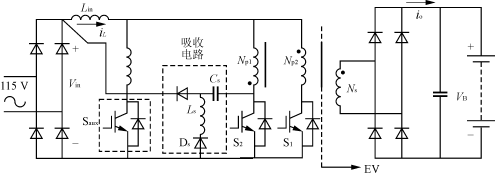
Figure 5 Isolated Boost Converter with Two Switch Tubes

Figure 6 voltage and current waveform
When the primary switching tubes S 1 and S 2 are both turned on, the energy is stored in the input filter inductor, and the output rectifier is in the off state. When the switch S S. 1 and transmitted to the primary winding 2 of any secondary switch off when a stored energy through. Due to the symmetrical operation of the converter, the transformer flux is reset and balanced.
In order to balance the input inductance volt-second product, it must be satisfied (1)
V inmax ≤ ![]() V B (1- D min ) (1)
V B (1- D min ) (1)
Assuming a transformer turns ratio of 1:1 and a maximum input voltage of 170V, the duty cycle is 0.15 for an output voltage of DC 200V and a duty cycle of 0.5 for an output voltage of DC 475V. As shown in Figure 5, the voltage stress on the main switch is 2 V B . When the output voltage is DC 400V, the switching tube voltage stress is DC 800V, and this voltage stress is quite high. Moreover, due to the leakage inductance of the transmission cable and inductive coupler, the device voltage stress may be higher. In order to limit the maximum voltage stress of the device, the lossless absorption circuit shown in Fig. 5 can be used. However, in either case, a 1200V voltage rating device must be used. Due to the high on-resistance of a high withstand voltage MOSFET, the conduction loss is large. Therefore, high voltage IGBTs with low conduction voltage drop should be considered. However, the switching losses of IGBT devices also limit the increase in switching frequency.
The average current of the switch is
I Savg = ![]() I L avg (2)
I L avg (2)
For a 1.5 kW power class, the input current is 15 A, the average switching current is 13 A, the peak current is 22 A, and a switching device with a current rating of at least 30 A is required. Although this scheme provides a relatively simple single-stage power conversion, there are also some drawbacks, such as high voltage stress on the semiconductor device, poor output voltage regulation performance, and large output current ripple.
In order to reduce the switching loss of the device, the soft switching circuit shown in Figure 5 can be used. The turn-off delay designed for the MOSFET ensures that the ZVS of the IGBT is turned off. In the current-up mode, the MOSFET shares the output filter current with half the voltage stress of the IGBT. Thus, a 600V device can be used. At the same time, the switching frequency is increased due to the reduction in turn-off loss.
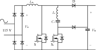
Another solution to reduce the device voltage rating is to use a two-stage conversion structure. The pre-stage PFC correction section can use a Boost converter with a soft switching function to allow high frequency operation. The latter stage DC/DC power conversion stage can use a half bridge series resonant converter to provide a high frequency current chain. Figure 7 shows a block diagram of a two-stage power conversion circuit suitable for charging mode 1.
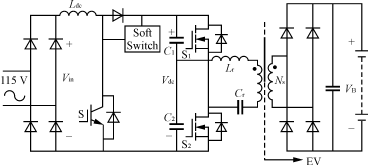
Figure 7 Two-stage power conversion circuit structure used in charging mode 1
If the input grid voltage is AC 115V, in order to reduce the current rating of the DC/DC converter, the output voltage can be increased to DC 450V. In this way, the Boost-level power switch can use a 500-600V MOSFET, and the half-bridge converter can use a 300-400V MOSFET. Due to the half bridge operation, the inductive coupler can use a 1:2 turns ratio. If the primary winding is 4 turns, the secondary winding is 8 turns. The current rating of the Boost switch is 30A, while the current rating of the half-bridge converter is 20A.
4.2 Charging mode 2
This is a normal charging mode for electric vehicles. The charging process is generally carried out in homes and public places, and requires a good user interface.
The charging power level of charging mode 2 is 6.6 kW. A standard grid power supply of 230V/30A size is sufficient to power this load. Its typical charging time is 5-8h.
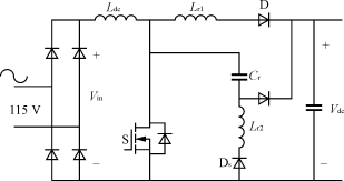
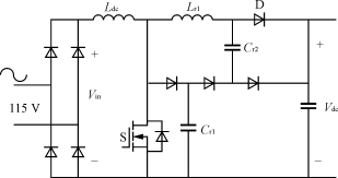
Similar to the charging power converter in charging mode 1, charging mode 2 can also employ a single-stage AC/DC converter. However, due to the single-stage converter with PFC function, the peak current of the switch tube is very high, so it is better to use a two-stage converter. Among them, the PFC stage can adopt the traditional Boost step-up type circuit, and the switch tube can be either a soft switch or a hard switch. However, in order to improve efficiency, it is more inclined to choose a soft-switching Boost converter. Figure 8 shows the power levels of the main circuit of a soft-open tube Boost converter using a lossless snubber circuit. Figure 9 shows two soft-switched Boost converter power stages using active-switch auxiliary circuits [7][8].
(a) One of the non-destructive absorption circuits
(b) Non-destructive absorption circuit 2
Figure 8. Soft-opening Boost converter with lossless absorption circuit
(a) ZCT
(b) ZVT
Figure 9 Soft-opening Boost converter power stage with active switching auxiliary circuit
If the grid input voltage is 230V, the output voltage can be adjusted to more than 400V. This makes the design of the post-stage converter easy, and the inductive coupler can take a 1:1 ratio. Therefore, if the maximum voltage of the battery is 400V, the output voltage of the front stage can be DC450V.
Compared to a soft-open Boost converter power stage with an additional active-switch auxiliary circuit, the lossless-amplified soft-opening Boost converter power stage is advantageous because it does not require active components. In particular, in Fig. 8(b), since the turn-off dv/dt of the switch is controlled, the turn-on voltage is turned on, and the voltage stress on the main switch is the output voltage, so that the performance of the whole machine is greatly improved. Figure 10 shows a typical waveform of a lossless absorption circuit.
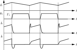
Figure 10 Typical waveform of a lossless absorption circuit
For a power rating of 6.6 kW, a 450V output voltage requires a 600V/60A MOSFET. According to the needs of the application, the whole machine design can choose single-module or multi-module parallel scheme.
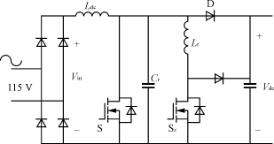
For the latter stage DC/DC converter, since the input and output are capacitive filters, only the high frequency converter with current source characteristics is suitable. The following topologies with large inductors in series with the primary side of the transformer are suitable for use. One of the forms is the full bridge type converter shown in FIG.
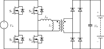
Figure 11 full bridge type charge converter
The series inductance is used in the primary circuit, so that the leakage inductance of the inductive coupler is effectively utilized, and the magnetizing inductance can also be utilized to expand the operating range of the converter ZVS. For the input bus voltage of 450V, a 1:1 turns ratio can be used, that is, the primary winding and the secondary winding are both 4 turns.
One of the disadvantages of the bridge topology of the converter topology is the high peak current, especially at low voltage inputs. In addition, when the light load is applied, the inverter enters the intermittent working state, the opening loss of the main switching tube increases, and the adjustment characteristics deteriorate. Therefore, it is usually necessary to ensure a minimum load current to ensure ZVS.
Another type of converter topology with high frequency current source characteristics is a resonant converter. These converter topologies are classified in the literature [8] and are divided into current and voltage types. In current mode converters, the converter is powered by a current source. In this type of topology, the current is effectively controlled. However, the drawback is that the voltage on the switch tube is not effectively controlled. Because most power devices are more resistant to overcurrent than overvoltage.
In addition, in voltage source converters, the voltage of the switching device is well limited, but in full-bridge and half-bridge topologies, it may be damaged by breakdown. These converters are generally classified into three types: series, parallel, and series-parallel resonance.
Figure 12 shows a schematic diagram of these basic resonant converter topologies. In a series resonant converter, the resonant inductor is connected in series with the primary side of the transformer, while in other types of converters, the capacitor is connected in series with the transformer. Only series resonant converters are hard current source characteristics, while other types of converters are hard voltage source types.
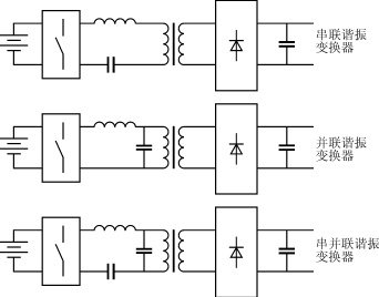
Figure 12 Resonant Converter Topology
In order to effectively utilize the inductive coupler magnetizing inductance and the interturn capacitance, different series resonant converters can be used. One topological form is the series-parallel LLCC resonant converter [9] [10] shown in FIG. Other resonant converters are also contemplated. As mentioned earlier, the turn-to-turn capacitance, magnetizing inductance, and leakage inductance are fully utilized. This solution is attractive because the converter and inductive coupler are well matched.
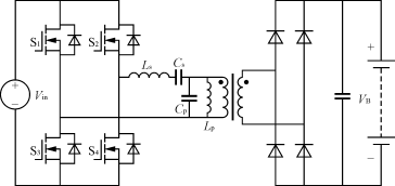
Figure 13 Series-parallel LLCC resonant converter
The converter can operate in a ZVS state above the resonant frequency, or in a ZCS state below the resonant frequency, as shown in FIG. The output voltage can be controlled by frequency conversion. However, in order to optimize the performance of the inductive coupler, it is generally designed that the high frequency corresponds to light load operation and the low frequency corresponds to heavy load operation, so that the switching loss of the converter remains substantially constant within the frequency variation range.
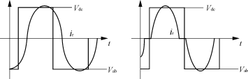
Figure 14 Two soft-switching modes of operation for series-parallel resonance
Due to the boosting characteristics of the parallel resonant circuit, the maximum converter voltage gain is slightly greater than one. For an input voltage of 450V and an output voltage of 400V, a 1:1 ratio can be used. The output voltage control characteristics of such a converter under light load operation are relatively poor, and other control techniques are required. One solution is to use the input Boost stage to regulate the output voltage, and the other is to use PWM or phase shift control. These two control techniques are described in more detail in the relevant literature.
4.3 Charging mode 3
This is a fast charging mode that focuses on charging for long distance travel. The charger corresponds to high power characteristics (>100kW) and is mainly used for some fixed charging stations. For a power rating of 100 kW, the charging time is approximately 15 min. In order to improve the power factor and reduce the input network harmonics, the converter input terminal generally needs to use an active rectifier circuit, as shown in Figure 15. Different control schemes can be used, including vector control, six-step wave control, digital control technology, etc. [11].
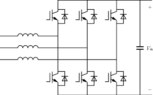
Figure 15 Active input rectifier circuit
In order to further improve the conversion efficiency and allow high frequency operation, a ZVT circuit as shown in Fig. 16 can be employed. The ZVT of the main switching device is realized by an auxiliary circuit, and the main switch is still PWM controlled.

Figure 16 ZVT three-phase boost rectification input circuit
As mentioned earlier, the high power charging mode is typically only used at the charging station. Because the charging station may be equipped with multiple chargers, each charger adopts a separate rectification stage, which inevitably makes the system bulky and the cost is greatly increased. To simplify the system design, the entire charging station can be equipped with a dedicated PFC or harmonic compensation converter, so that the charging main circuit is connected to the same active input rectifier circuit, as shown in Figure 17.
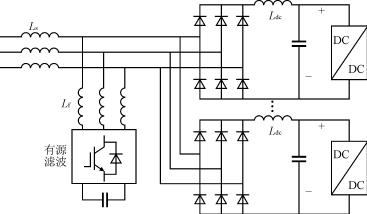
Figure 17 Main circuit structure of a charger system equipped with a dedicated PFC or harmonic compensator
The active filter rating is approximately 20% of the rated power rating of the charging station. The DC side inductor is generally used at the rectifying end to increase the power factor of the rectifier, and an active filtering scheme in series or parallel mode can be selected.
The active filter can use a traditional hard-switching PWM inverter circuit or a soft-switching inverter to operate at a higher switching frequency, increase the control bandwidth, and compensate for higher-order harmonics. The resonant DC link converter is more suitable for operation in a wide range of medium power range inverters. Figure 18 shows the active clamp resonant DC link inverter power circuit.
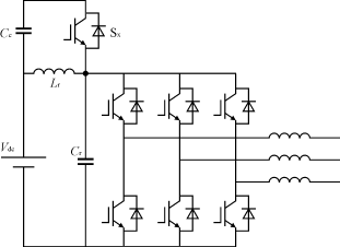
Figure 18 Active clamped resonant DC link inverter power circuit
Different from the traditional PWM converter, the resonant DC link inverter adopts Discrete Pulse Modulation (DPM) control, and the switching frequency is high, and the required filter size is small. In addition, since d v /d t is controlled, the generated EMI is small.
Similar to charging mode 2, the charging converter can directly use a full bridge or a full bridge converter with resonance. However, due to the higher power stage of the charging mode 3, a general full-bridge converter necessarily corresponds to a very high peak current compared to a resonant full-bridge converter. Therefore, ZVS or ZCS resonant full-bridge topology should be considered to effectively reduce losses.
As mentioned earlier, the series-parallel full-bridge resonant converter is an optional topology that satisfies all design considerations for inductively coupled charge converters and fully utilizes the equivalent circuit components of the inductive coupler. Depending on the performance of the power device, the ZVS or ZCS scheme can be selected separately.
For high power and high frequency applications, IGBTs with relatively small conduction losses and high frequency capability are more attractive. Since the inductive coupler is optimized for a frequency range of 70 to 300 kHz, soft switching techniques are needed to optimize the performance of the IGBT. The results in [10] show that in the case of ZVS, the IGBT turn-off loss is still large and the die temperature is high; while ZCS can turn off the IGBT in the ZCS case, reducing the turn-off loss and making the IGBT more capable. Good for high switching frequencies.
To further reduce the device current stress and reduce the size and weight of the transmission cable, a higher level of bus voltage can be used. Inductive couplers can now have a 2:1 turns ratio. Therefore, when the secondary side adopts 4 turns, the primary side must adopt 8 turns. For a battery voltage of 400V, the DC bus voltage must be at least DC800V. In this case, an IGBT with a rating of 1200V/400A must be used.
5 Conclusion
In this paper, the charger for electric vehicle battery is discussed in accordance with SAEJ-1773's provisions for inductive couplers. According to the standard of the inductive coupler and different charging modes, several design schemes of the charger matched with the inductive coupler are determined, and the circuit topology suitable for different charging modes is selected. Finally, alternative converter topology schemes suitable for different charging levels are presented.
Belttt's Low Frequency Inverter also call industrial frequency inverter. It's the heavy duty inverter and has broader fields of application. Our Low Frequency UPS inverters are build-in strong impact resistance. The switching time between city power and your batteries is less than 10ms. To protect your batteries, we also build-in three-stage charging mode.
Low Frequency UPS
Frequency Inverter,Car Inverter,Low Frequency Inverter,Low FrequencyPS
Guangzhou City Poojin Electronic Technology Co., Ltd. , http://www.inverter-belttt.com