Abstract: The following arTIcle describes how to slow down and store high-speed data of a typical flash data converter such as the MAX101A. This note also provides helpful guidance for PCB layout, TIming informaTIon and a simple test circuit to evaluate the performance of the ADC, while at the same TIme testing the functionality of the FIFO memory design.
Fast data-acquisition systems and other high-speed applications convert analog signals to digital word streams as a prerequisite to the extraction or demodulation of information. To properly apply the A / D converter in these applications, you should understand its dynamic parameters, the circuit layout, and the available methods for storing high-speed digital data.
This article describes the MAX101A A / D converter and evaluation kit along with the interface and PC-layout considerations necessary for high-frequency operation. In particular, it presents a memory-storage concept valuable for high-speed data-acquisition systems. The special technique has been tested and proven with digitized data from a high-speed ADC. MAX101A: The Data-Acquisition WorkhorseThe MAX101A flash ADC resides in a special package that includes a track / hold amplifier (T / H) with 1.2GHz input bandwidth, and a quantizer of proprietary design that achieves excellent dynamic performance available in current 8-bit, 500Msps A / D converters. Careful T / H design is vital in achieving this performance. The T / H amplifier resides on a separate chip fabricated with Maxim's junction- isolated SH3 process, and its laser-trimmed 50Ω differential inputs accept full-scale amplitudes of ± 125mV differential or ± 250mV single-ended.
When the sampling clock is high, the input amplifier buffers and drives the hold capacitor. With the sampling clock transitioning low, the sampling bridge closes (within an interval known as the "aperture delay") and allows the resulting analog value to be held and presented to the quantizer. The T / H circuit also buffers the applied differential clock signal and feeds it to the quantizer. The converter sports a 7.2 effective number of bits (ENOB) at the 250MHz Nyquist frequency, an excellent value made possible by the T / H's wide -3dB bandwidth (greater than 1.2GHz). Even when undersampling a 600MHz input tone at 500Msps, this unique T / H circuit achieves an ENOB greater than 6.8.
The MAX101A's two time-interleaved quantizers, each consisting of two voltage-interleaved 7-bit flash stages, are manufactured with Maxim's 27GHz GST-2 bipolar process. Each stage has an independent reference-resistor string driven by an external, user-supplied reference buffer. Interleaved 7-bit stages give the MAX101A a very low rate of metastable error (less than one error per 1018 conversions), which in turn provides low THD and superior AC linearity. A bias pin lets the user optimize performance by adjusting relative sample times for the two interleaved converters.
The MAX101A's two 8-bit, single-ended output ports have been made ECL-compatible to accommodate high-speed data streams, however most memories used with the MAX101A are TTL-compatible. ECL-to-TTL-level shifters must therefore be introduced to adjust the signal levels before they are applied to the RAM chips.
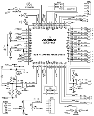
Proper packaging is essential to the performance of high-speed ADCs. The MAX101A package is an 84-lead, multilayer, nonhermetic, ceramic type whose stripline architecture closely controls the run impedance from die to die and from each die to the external package pins. The junction-to-ambient thermal resistance (Θ) is approximately 12 ° C / W with proper cooling (200ft / min), which can be achieved with a combination of heatsink and (ideally) an external fan. A simple cooling fan for computer power supplies does the job when mounted on top of a heatsink attached to the bottom of the chip. PC-Layout and Power-Supply Considerations for the MAX101AEVKITIn addition to dynamic parameters, the factors of importance to high-speed ADC users include cost, power dissipation, input-signal conditioning, and proper PC layout. An excellent example of high-quality layout is the MAX101A evaluation board (Figure 1).
For Larger Image
Figure 1. MAX101A core design of the evaluation board.
The evaluation kit's multilayer board exhibits special attention to layout. Containing high-speed analog and digital circuitry for evaluating the flash converter's initial performance, it has 16 data outputs (two 8-bit words) and a data-clock output. In conjunction with the MAX101A, it specifies data rates up to 500Msps. The board accommodates an external clock source via an SMA connector and accepts analog inputs (AIN + and AIN-) via two other SMA connectors. Each analog input connects directly to the ADC with 50Ω terminations internal to the MAX101A.
A separate termination board with 50Ω ECL pulldown resistors is included with the kit. Connected to the main board with a 3x32-pin EURO-card connector, it provides proper ECL termination along with access to the converter's output data. The termination board also features data -clock outputs and two square pin headers, each providing eight data outputs. A high-speed logic analyzer (eg HP16500C) lets you observe either AData or BData.
The MAX101A main evaluation board comes fully assembled and tested with the MAX101A installed and requires standard power supplies of + 5V and -5.2V. This power can be supplied through the 3x32 EURO-card connector or through pads on the edge of the board. Nominal power dissipation for main and termination board combined is 17W. To simplify PC layout and circuit design, you can integrate the MAX101AEVKIT into your system as a modular subsystem.
Because digital circuits are excellent generators of electromagnetic interference, a multilayer PC board is recommended for high-speed components like the MAX101A. Clock signals and other high-frequency square waves are rich in harmonics that can invade the entire application, and higher harmonic frequencies can Even excite a resonance between the cable and the PC traces. The MAX101A evaluation board consists of six layers of circuitry (ground, power, analog, and digital) separated by five layers of epoxy (Table 1).
Table 1. Layer-Thickness Profile for the MAX101AEVKIT
* MR is the microstrip return.
To minimize the effects of interference, digital and analog grounds should be tied to a single "star connection" close to the power-supply source. As an example, the MAX101AEVKIT's digital ground ties to analog ground at a ferrite-bead suppressor. Another ferrite bead between the digital power (VEE) and -5.2V analog power (VAA) helps to decouple the power rails.
The best approach for preventing RF interference is keeping the layout traces short and avoiding extra resonance loops. Short traces minimize conductor impedance and shorten signal-propagation delays, which measure about 5.7ps / mm (145ps / inch). Because prop delay is an important consideration in operating the high-speed MAX101A, Maxim recommends that trace lengths not exceed 0.5 inches (12mm). Though it limits the maximum delay to 70ps for each trace, this condition cannot always be achieved. In some cases it's more important for corresponding lines to be of equal length and terminated correctly.
Controlled-impedance transmission-line connections are recommended for analog inputs, clock signals, and fast digital outputs. The MAX101AEVKIT, for instance, employs microstrip lines with various values ​​of characteristic impedance. The ADC's data outputs drive differential line drivers through 100Ω microstrip lines occupying layers 1 and 3, and 50Ω microstrip lines, which occupy layers 1 and 2. Table 1 features a profile of the nominal thicknesses required for each layer of foil and dielectric material. To achieve full speed, low noise, and high-quality operation in a multilayer-interconnect design, trace widths should be 500µm for 50Ω microstrip lines and 250µm for 100Ω microstrip lines. Interfacing the MAX101A to External Memory When clocked at 500MHz, the MAX101A produces 250MHz at each of the two interleaved ports A and B. This digitized data is synchronized to the DCLK signal (port A to the falling edge and port B to the rising edge). DCLK can also clock a D-type flip-flop f or storing data. The major difficulty in this design is storing the data in a conventional memory. The following section provides a practical and fully tested solution to that problem.
Figure 2 shows the simplified version of a technique for storing MAX101A data in external FIFO registers. Each MAX101A port is connected to a single 8-bit D-type storage register whose outputs are valid for nearly 4ns. Buffer registers at port A and port B drive two high-speed buses that are terminated with resistor networks matching the line impedance.
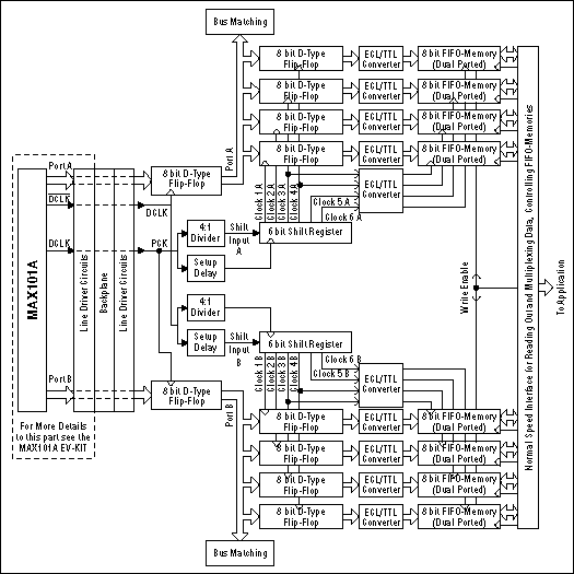
Figure 2. Data storage concept for a MAX101A-RAM combination.
Each input register drives four other D-type registers in parallel. The rather insignificant time delay introduced by these registers is not an issue, because their clock signal is derived from an edge opposite to the edge driving the input-register clock. The circuitry associated with port A and port B is identical, so the timing of clock and data signals will remain correct if the corresponding PC traces are of similar length and geometry. Gate delays in Figure 2 have the following relationship:
ΔtSHIFT REGISTER + tSETUP DELAY-ΔtINPUT REGISTER + tSETUP FOR DATA D-FLIP-FLOPS ≤ 2ns
To control the four data registers on the high-speed bus, the 250MHz synchronization signals PCK and NCK are first divided by four and then applied to a 6-bit shift register. The clock signals NCK and PCK are also slowed by one gate delay each to compensate for the 4: 1 divider delay and the shift register's setup time. Good results can be achieved using an AND gate for each of these delays.
Division by four produces a 62.5MHz clock signal that shifts through the dedicated register, producing identical-waveform outputs that emerge at 4ns intervals. These signals have the proper sequence for clocking incoming data to the proper data registers. To match the data registers' ECL -compatible outputs with the high-capacity FIFOs 'TTL-compatible inputs, the ECL-to-TTL converter's delay must be compensated for without violating the FIFOs' setup time. Thanks to the delay in the ECL-to-TTL converters, each shift -register output connects to the FIFO two bit-intervals later than does the corresponding data-register output. This arrangement, in which each output period is 16ns long (equivalent to four bit-intervals in the shift register), meets the timing requirements of Figure 3.
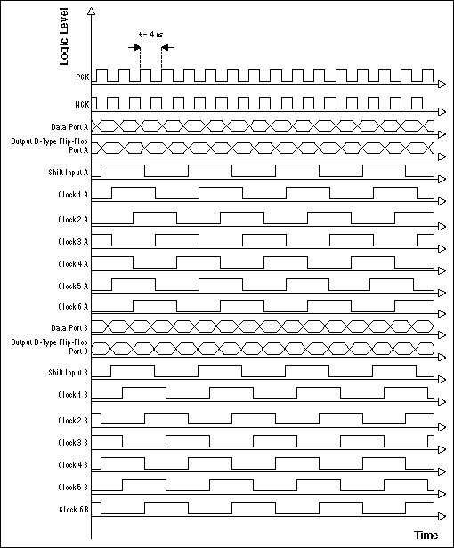
Figure 3. Timing for RAM selection.
The FIFOs' Write_Enable signals allows for scanning continuously or for triggering a burst of data. The FIFO configuration discussed in this article allows memory depths to 32kbytes and more. For data scans in the Mbyte range, however, this data-storage method must be modified or substituted by another technique.
Timing requirements for the FIFO memory are similar to those of the MAX101A outputs. When data is valid at a FIFO input, a positive Write_Clock edge takes it into the memory. A high-speed bus interconnects the four data registers. Operating at 15.625MHz, they require new data every 64ns. This relatively long interval enables the use of a conventional, high-capacity SRAM memory. After the ECL-to-TTL conversion, the data rate is sufficiently low that state-of-the-art programmable logic devices Can take it from there. Instead of FIFO memory, for example, an FPGA could provide the interface to external static RAM devices. Though not tested, this approach (using 512kx8 SRAM devices) would allow memory depths to 16Mbytes. Determining ADC LinearityAmong the tests performed on the Figure 2 circuit was a test of the ADC's linearity. The logic analyzer used in preliminary divide-by-10 tests was not able to keep up with the MAX101A at full speed, so the high-speed data acquisition system in its f inal form was used to successfully test and confirm the ADC's excellent linearity.
For that experiment (Figure 4), a constant voltage from a quality voltage source (Gossen-Metrawatt) was fed through a 1kΩ resistor to the MAX101A's SMA input. A Hewlett Packard precision multimeter (HP3438A) monitored signal voltage. The MAX101A requires an input voltage between -250mV to + 250mV. The results show excellent linearity for the high-speed core of the application.
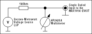
Figure 4. Configuration for MAX101A linearity test.
The MAX101A full-scale input range (FSR) is apparent from a diagram of input voltage versus output code (Table 2 and Figure 5). Representing a MAX101A operating in single-ended mode, this diagram shows the output codes corresponding to an input voltage taken through the entire FSR. The binary zero output (00000000) occurs at -250mV. The midscale output (01111101) indicates a slight error when compared with the ideal binary output for midscale (10000000). Full scale (+ 250mV) produces an output code of 11110101, again indicating a slight deviation with respect to the ideal output (11111111). These deviations are caused by an offset that can be compensated within the application if necessary.
Table 2. MAX101A Input Ranges
* An offset VIO is present at the input, as specified in the MAX101A data sheet's DC Electrical Characteristics. This offset can be compensated by adjusting the reference voltages or by introducing an offset voltage at one of the input terminals AIN + or AIN-.
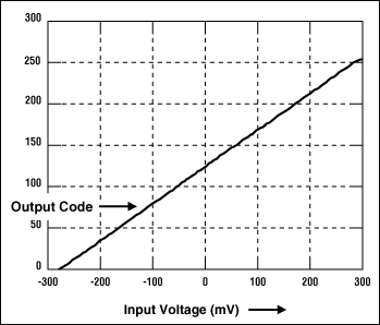
Figure 5. MAX101A linearity function (VIN vs. OUTBIN).
Successful high-frequency applications require excellent dynamic performance, high-quality layout, and proper attention to signal conditioning and power consumption. The MAX101A with its unique combination of T / H amplifier and quantizer ensures these attributes, as does its successor, the 8- bit, 1Gsps MAX104. The MAX104's high sample rate and 2.2GHz differential T / H amplifier represents current state-of-the-art performance for 8-bit A / D converters. Integrated Analog-to-Digital and Digital-to-Analog Converters . Van de Plassche, Rudy. Philips Research Laboratories, Eindhoven, Netherlands, KAP 1994.
The Art of Electronics. Horowitz, Paul and Hill, Winfield. Cambridge University Press, 1989, 2nd Edition, New York.
MAX101 / MAX101A Evaluation Kit data sheet. Maxim Integrated Products Inc., USA, 1996.
MAX101A data sheet. Maxim Integrated Products Inc., USA, 1996. A similar version of this article appeared in the June 1998 issue of Microwaves & RF.
Fast data-acquisition systems and other high-speed applications convert analog signals to digital word streams as a prerequisite to the extraction or demodulation of information. To properly apply the A / D converter in these applications, you should understand its dynamic parameters, the circuit layout, and the available methods for storing high-speed digital data.
This article describes the MAX101A A / D converter and evaluation kit along with the interface and PC-layout considerations necessary for high-frequency operation. In particular, it presents a memory-storage concept valuable for high-speed data-acquisition systems. The special technique has been tested and proven with digitized data from a high-speed ADC. MAX101A: The Data-Acquisition WorkhorseThe MAX101A flash ADC resides in a special package that includes a track / hold amplifier (T / H) with 1.2GHz input bandwidth, and a quantizer of proprietary design that achieves excellent dynamic performance available in current 8-bit, 500Msps A / D converters. Careful T / H design is vital in achieving this performance. The T / H amplifier resides on a separate chip fabricated with Maxim's junction- isolated SH3 process, and its laser-trimmed 50Ω differential inputs accept full-scale amplitudes of ± 125mV differential or ± 250mV single-ended.
When the sampling clock is high, the input amplifier buffers and drives the hold capacitor. With the sampling clock transitioning low, the sampling bridge closes (within an interval known as the "aperture delay") and allows the resulting analog value to be held and presented to the quantizer. The T / H circuit also buffers the applied differential clock signal and feeds it to the quantizer. The converter sports a 7.2 effective number of bits (ENOB) at the 250MHz Nyquist frequency, an excellent value made possible by the T / H's wide -3dB bandwidth (greater than 1.2GHz). Even when undersampling a 600MHz input tone at 500Msps, this unique T / H circuit achieves an ENOB greater than 6.8.
The MAX101A's two time-interleaved quantizers, each consisting of two voltage-interleaved 7-bit flash stages, are manufactured with Maxim's 27GHz GST-2 bipolar process. Each stage has an independent reference-resistor string driven by an external, user-supplied reference buffer. Interleaved 7-bit stages give the MAX101A a very low rate of metastable error (less than one error per 1018 conversions), which in turn provides low THD and superior AC linearity. A bias pin lets the user optimize performance by adjusting relative sample times for the two interleaved converters.
The MAX101A's two 8-bit, single-ended output ports have been made ECL-compatible to accommodate high-speed data streams, however most memories used with the MAX101A are TTL-compatible. ECL-to-TTL-level shifters must therefore be introduced to adjust the signal levels before they are applied to the RAM chips.
Proper packaging is essential to the performance of high-speed ADCs. The MAX101A package is an 84-lead, multilayer, nonhermetic, ceramic type whose stripline architecture closely controls the run impedance from die to die and from each die to the external package pins. The junction-to-ambient thermal resistance (Θ) is approximately 12 ° C / W with proper cooling (200ft / min), which can be achieved with a combination of heatsink and (ideally) an external fan. A simple cooling fan for computer power supplies does the job when mounted on top of a heatsink attached to the bottom of the chip. PC-Layout and Power-Supply Considerations for the MAX101AEVKITIn addition to dynamic parameters, the factors of importance to high-speed ADC users include cost, power dissipation, input-signal conditioning, and proper PC layout. An excellent example of high-quality layout is the MAX101A evaluation board (Figure 1).
For Larger Image
Figure 1. MAX101A core design of the evaluation board.
The evaluation kit's multilayer board exhibits special attention to layout. Containing high-speed analog and digital circuitry for evaluating the flash converter's initial performance, it has 16 data outputs (two 8-bit words) and a data-clock output. In conjunction with the MAX101A, it specifies data rates up to 500Msps. The board accommodates an external clock source via an SMA connector and accepts analog inputs (AIN + and AIN-) via two other SMA connectors. Each analog input connects directly to the ADC with 50Ω terminations internal to the MAX101A.
A separate termination board with 50Ω ECL pulldown resistors is included with the kit. Connected to the main board with a 3x32-pin EURO-card connector, it provides proper ECL termination along with access to the converter's output data. The termination board also features data -clock outputs and two square pin headers, each providing eight data outputs. A high-speed logic analyzer (eg HP16500C) lets you observe either AData or BData.
The MAX101A main evaluation board comes fully assembled and tested with the MAX101A installed and requires standard power supplies of + 5V and -5.2V. This power can be supplied through the 3x32 EURO-card connector or through pads on the edge of the board. Nominal power dissipation for main and termination board combined is 17W. To simplify PC layout and circuit design, you can integrate the MAX101AEVKIT into your system as a modular subsystem.
Because digital circuits are excellent generators of electromagnetic interference, a multilayer PC board is recommended for high-speed components like the MAX101A. Clock signals and other high-frequency square waves are rich in harmonics that can invade the entire application, and higher harmonic frequencies can Even excite a resonance between the cable and the PC traces. The MAX101A evaluation board consists of six layers of circuitry (ground, power, analog, and digital) separated by five layers of epoxy (Table 1).
Table 1. Layer-Thickness Profile for the MAX101AEVKIT
| Layer Type | Material | Thickness | Dielectric Constant | Layer Level | |
| Dielectric | FR4 Epoxy | 280µm | 4.1 to 4.9 | 1-2, 2-3, 3-4, 4-5, 5-6 | |
| Copper | Copper Foil | 35.5µm | ----- | Microstrip Signals | 1 |
| 50Ω MR * GND Plane | 2 | ||||
| 100Ω MR * GND Plane | 3 | ||||
| VCC / VTT Power Plane | 4 | ||||
| VEE / VAA Power Plane | 5 | ||||
| DC Signal | 6 | ||||
* MR is the microstrip return.
To minimize the effects of interference, digital and analog grounds should be tied to a single "star connection" close to the power-supply source. As an example, the MAX101AEVKIT's digital ground ties to analog ground at a ferrite-bead suppressor. Another ferrite bead between the digital power (VEE) and -5.2V analog power (VAA) helps to decouple the power rails.
The best approach for preventing RF interference is keeping the layout traces short and avoiding extra resonance loops. Short traces minimize conductor impedance and shorten signal-propagation delays, which measure about 5.7ps / mm (145ps / inch). Because prop delay is an important consideration in operating the high-speed MAX101A, Maxim recommends that trace lengths not exceed 0.5 inches (12mm). Though it limits the maximum delay to 70ps for each trace, this condition cannot always be achieved. In some cases it's more important for corresponding lines to be of equal length and terminated correctly.
Controlled-impedance transmission-line connections are recommended for analog inputs, clock signals, and fast digital outputs. The MAX101AEVKIT, for instance, employs microstrip lines with various values ​​of characteristic impedance. The ADC's data outputs drive differential line drivers through 100Ω microstrip lines occupying layers 1 and 3, and 50Ω microstrip lines, which occupy layers 1 and 2. Table 1 features a profile of the nominal thicknesses required for each layer of foil and dielectric material. To achieve full speed, low noise, and high-quality operation in a multilayer-interconnect design, trace widths should be 500µm for 50Ω microstrip lines and 250µm for 100Ω microstrip lines. Interfacing the MAX101A to External Memory When clocked at 500MHz, the MAX101A produces 250MHz at each of the two interleaved ports A and B. This digitized data is synchronized to the DCLK signal (port A to the falling edge and port B to the rising edge). DCLK can also clock a D-type flip-flop f or storing data. The major difficulty in this design is storing the data in a conventional memory. The following section provides a practical and fully tested solution to that problem.
Figure 2 shows the simplified version of a technique for storing MAX101A data in external FIFO registers. Each MAX101A port is connected to a single 8-bit D-type storage register whose outputs are valid for nearly 4ns. Buffer registers at port A and port B drive two high-speed buses that are terminated with resistor networks matching the line impedance.
Figure 2. Data storage concept for a MAX101A-RAM combination.
Each input register drives four other D-type registers in parallel. The rather insignificant time delay introduced by these registers is not an issue, because their clock signal is derived from an edge opposite to the edge driving the input-register clock. The circuitry associated with port A and port B is identical, so the timing of clock and data signals will remain correct if the corresponding PC traces are of similar length and geometry. Gate delays in Figure 2 have the following relationship:
ΔtSHIFT REGISTER + tSETUP DELAY-ΔtINPUT REGISTER + tSETUP FOR DATA D-FLIP-FLOPS ≤ 2ns
To control the four data registers on the high-speed bus, the 250MHz synchronization signals PCK and NCK are first divided by four and then applied to a 6-bit shift register. The clock signals NCK and PCK are also slowed by one gate delay each to compensate for the 4: 1 divider delay and the shift register's setup time. Good results can be achieved using an AND gate for each of these delays.
Division by four produces a 62.5MHz clock signal that shifts through the dedicated register, producing identical-waveform outputs that emerge at 4ns intervals. These signals have the proper sequence for clocking incoming data to the proper data registers. To match the data registers' ECL -compatible outputs with the high-capacity FIFOs 'TTL-compatible inputs, the ECL-to-TTL converter's delay must be compensated for without violating the FIFOs' setup time. Thanks to the delay in the ECL-to-TTL converters, each shift -register output connects to the FIFO two bit-intervals later than does the corresponding data-register output. This arrangement, in which each output period is 16ns long (equivalent to four bit-intervals in the shift register), meets the timing requirements of Figure 3.
Figure 3. Timing for RAM selection.
The FIFOs' Write_Enable signals allows for scanning continuously or for triggering a burst of data. The FIFO configuration discussed in this article allows memory depths to 32kbytes and more. For data scans in the Mbyte range, however, this data-storage method must be modified or substituted by another technique.
Timing requirements for the FIFO memory are similar to those of the MAX101A outputs. When data is valid at a FIFO input, a positive Write_Clock edge takes it into the memory. A high-speed bus interconnects the four data registers. Operating at 15.625MHz, they require new data every 64ns. This relatively long interval enables the use of a conventional, high-capacity SRAM memory. After the ECL-to-TTL conversion, the data rate is sufficiently low that state-of-the-art programmable logic devices Can take it from there. Instead of FIFO memory, for example, an FPGA could provide the interface to external static RAM devices. Though not tested, this approach (using 512kx8 SRAM devices) would allow memory depths to 16Mbytes. Determining ADC LinearityAmong the tests performed on the Figure 2 circuit was a test of the ADC's linearity. The logic analyzer used in preliminary divide-by-10 tests was not able to keep up with the MAX101A at full speed, so the high-speed data acquisition system in its f inal form was used to successfully test and confirm the ADC's excellent linearity.
For that experiment (Figure 4), a constant voltage from a quality voltage source (Gossen-Metrawatt) was fed through a 1kΩ resistor to the MAX101A's SMA input. A Hewlett Packard precision multimeter (HP3438A) monitored signal voltage. The MAX101A requires an input voltage between -250mV to + 250mV. The results show excellent linearity for the high-speed core of the application.
Figure 4. Configuration for MAX101A linearity test.
The MAX101A full-scale input range (FSR) is apparent from a diagram of input voltage versus output code (Table 2 and Figure 5). Representing a MAX101A operating in single-ended mode, this diagram shows the output codes corresponding to an input voltage taken through the entire FSR. The binary zero output (00000000) occurs at -250mV. The midscale output (01111101) indicates a slight error when compared with the ideal binary output for midscale (10000000). Full scale (+ 250mV) produces an output code of 11110101, again indicating a slight deviation with respect to the ideal output (11111111). These deviations are caused by an offset that can be compensated within the application if necessary.
Table 2. MAX101A Input Ranges
| Input | AIN + (mV) * | AIN- (mV) * | Output Code | MSB to LSB |
| Differential | +125 | -125 | 11111111 | Full Scale |
| 0 | 0 | 10000000 | Midscale | |
| -125 | +125 | 00000000 | Zero Scale | |
| Single-Ended | +250 | 0 | 11111111 | Full Scale |
| 0 | 0 | 10000000 | Midscale | |
| -250 | 0 | 00000000 | Zero Scale |
* An offset VIO is present at the input, as specified in the MAX101A data sheet's DC Electrical Characteristics. This offset can be compensated by adjusting the reference voltages or by introducing an offset voltage at one of the input terminals AIN + or AIN-.
Figure 5. MAX101A linearity function (VIN vs. OUTBIN).
Successful high-frequency applications require excellent dynamic performance, high-quality layout, and proper attention to signal conditioning and power consumption. The MAX101A with its unique combination of T / H amplifier and quantizer ensures these attributes, as does its successor, the 8- bit, 1Gsps MAX104. The MAX104's high sample rate and 2.2GHz differential T / H amplifier represents current state-of-the-art performance for 8-bit A / D converters. Integrated Analog-to-Digital and Digital-to-Analog Converters . Van de Plassche, Rudy. Philips Research Laboratories, Eindhoven, Netherlands, KAP 1994.
The Art of Electronics. Horowitz, Paul and Hill, Winfield. Cambridge University Press, 1989, 2nd Edition, New York.
MAX101 / MAX101A Evaluation Kit data sheet. Maxim Integrated Products Inc., USA, 1996.
MAX101A data sheet. Maxim Integrated Products Inc., USA, 1996. A similar version of this article appeared in the June 1998 issue of Microwaves & RF.
With the continuous maturity of LED lighting technology, the automotive industry has been using LED light sources for instrument panels and interior lighting, and LED lighting is gradually capturing brake lights, fog lights, low beam lights, high beam lights, and daytime running lights. Application fields such as adaptive headlights (AFS) for exterior signal indication and headlight illumination.The challenge for LEDs to be used in exterior lighting is the need for integrated, flexible and networked drives.
Automotive Pcb,Blank Circuit Board,Metal Core Pcb,Power Circuit Board
Chuangying Electronics Co.,Ltd , https://www.cwpcb.com