In the past car audio system design, the highest clock frequency on a PCB is already very high at 30~50MHz, and now most PCB clock frequencies exceed 100MHz, and some even reach the order of GHz. For this reason, the traditional serial-driven serial design method can no longer meet today's design requirements. Now it is necessary to adopt a newer design concept and design method, that is, the serial design process driven by the netlist will be changed to the whole Design a parallel process in which all aspects are considered in parallel. That is to say, the design requirements and constraints that were only considered in the PCB layout and wiring stages in the past will be given enough attention and evaluation in the schematic design stage. At the beginning of the design, the selection of key devices will be analyzed, and the key network cables will be conceived. Topology, termination of matching network settings, and full consideration of the PCB stack structure before wiring begins, reducing crosstalk between signals to ensure power integrity and timing.
This paper mainly introduces the high-speed DDR200 used in car audio navigation systems. Under the guidance of the basic theory and professional design experience of high-speed circuits, the PCB design method to ensure signal integrity.
1 What is DDR and its basic working principle
DDR SDRAM, accustomed to be called DDR.DDR SDRAM, double-rate synchronous dynamic random access memory.
DDR memory is based on SDRAM memory. SDRAM transfers data only once in one clock cycle. It transmits data during the rising period of the clock. DDR memory transfers data twice in one clock cycle. It can transmit data once during the rising and falling phases of the clock. Therefore, it is called double rate synchronous dynamic random access memory. DDR memory can achieve double data transfer rates at the same bus frequency as SDRAM.
As shown in Figure 1 and Figure 2 below, DDR SDRAM has two more signals than SDRAM: CLK# and DQS. 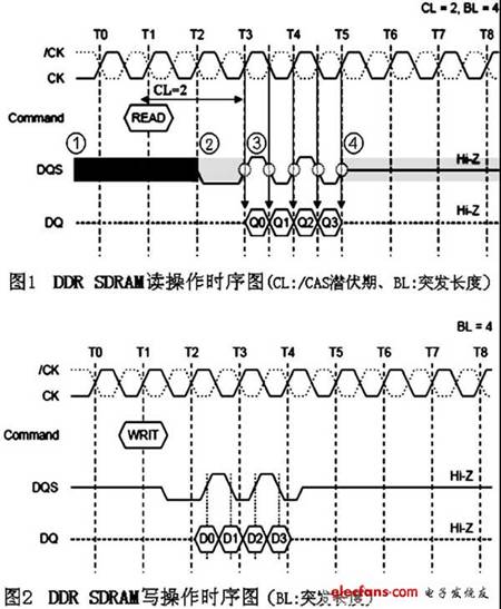
CLK# is opposite to the normal CLK clock phase and forms a differential clock signal. The data transmission is performed at the intersection of CLK and CLK#, that is, data is triggered on the rising and falling edges of CLK (which is exactly the rising edge of CLK#), thereby achieving double rate transmission.
DQS (DQ STrobe, data selection pulse) is an important function in DDRSDRAM. It is mainly used to accurately distinguish each transmission period in one clock cycle, and use DQS to read the corresponding data DQ at the receiving end.
DQS is active on both rising and falling edges and is generated simultaneously with the data signal. Both DQS and DQ are two-way signals that are transmitted bidirectionally. During a read operation, the edge of the DQS signal is aligned in timing with the edge of the signal at DQ, while the edge of the DQS signal is aligned in time with the center of the DQ signal during a write operation.
The following is an example of the 1-DDR SDRAM read operation timing diagram to illustrate the control principle of DQS:
1 DQS is at a high impedance level when there is no data output.
2 After receiving the READ command, the DQS signal becomes low impedance and is one cycle ahead of the data output time.
3 The DQS signal is generated simultaneously with the data signal at the intersection of CLK and CLK#, and the frequency is the same as CLK.
The 4DQS signal continues until the burst of the read pulse is completed, and then returns to the high impedance level after completion.
2 Basic specifications
Basic specifications for DDR SDRAM (Table 1).
Table 1 Basic specifications of DDR SDRAM 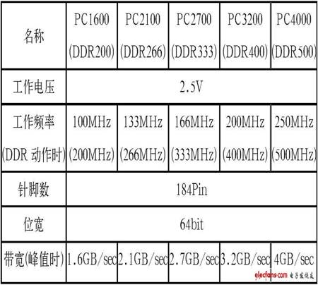
This article refers to the address: http://
3 DDR200 PCB design method
The DDR200 used in the car audio navigation system is taken as an example to consider the PCB design method from the aspects of PCB stack structure selection, wiring topology, crosstalk, power integrity and timing.
3.1 PCB laminate structure selection
The laminated structure of the circuit board directly determines the transmission speed and delay time of the signal in each conductor layer. Depending on the circuit configuration and structural constraints, combined with the EMI requirements of the high-speed signal and the return path of the power supply, it is important to determine the laminated structure and the wiring layer of important signals at the initial stage of design. The laminated structure of this example and the wiring layer of important signals are shown in Fig. 3.
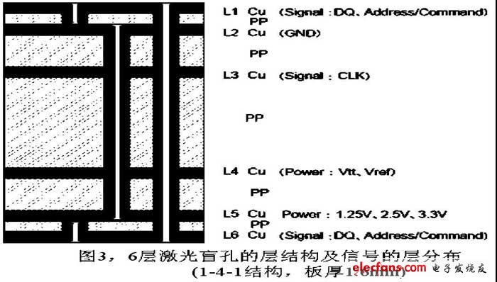
Depending on the sheet material, the thickness of the conductor copper, the thickness of each insulating layer, and the dielectric constant may vary, resulting in a difference in the characteristic impedance Zo and the propagation delay Tpd of the high-speed signal transmission line.
The dielectric constant of the insulating medium in the sheet is εr=4.0, the thickness of the insulating layer is PP1=60μm, PP2=200μm, PP3=800μm, the thickness of the conductor copper is 35μm, and the line width W=100μm, the signal is transmitted in the surface layer (L1, L6). The delay time is Tpd≒140ps, the characteristic impedance is Zo≒56Ω, the transmission delay of the inner layer L3 wiring is Tpd≒170ps, and the characteristic impedance is Zo≒84Ω.
3.2 DDR SDRAM signal wiring standards
In order to control the effects of the impedance and delay of the transmission line, the following wiring design criteria must be determined:
* High-speed signal line width to ensure the transmission line characteristic impedance value: differential signal Zo 100Ω, other signals Zo ≒ 50Ω.
* To reduce crosstalk between transmission lines, determine the minimum spacing value. Increase the spacing as much as possible during actual wiring.
* Hole diameter and via pad diameter of available vias:
1Build-up laminated laser punching hole 2 inner blind buried hole (used by L2 to L5) 3 through hole (for L1 to L6) 4 minimum spacing between various via pads.
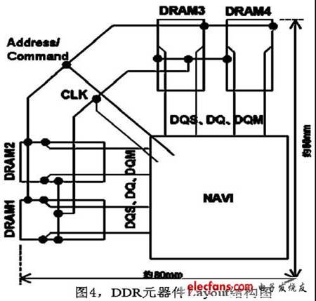
3.3 DDR SDRAM device layout structure
The data transmission of DDR is usually a structure in which one transmitting end corresponds to multiple receiving ends. In order to realize synchronous transmission of data, the control of delay time is particularly important. When constructing the device layout, it is important to consider the selection of the transmission line divergence nodes, the length of each segment, and so on. As shown in Figure 4, the components in the DDR-related circuit are placed on the same surface, and the "Star and Y-type topologies" are used to implement CLK, Data data groups, and data groups such as Address/Command. Long wiring control.
3.4 High-frequency signal routing priority
According to the strictness of the design requirements, start from the most important signal lines, in the order:
CLK→Data→Address/Command
3.5 CLK differential signal wiring method
For the CLK differential signal used in DDR200, the wiring topology is shown in Figure 5. The wiring notes are as follows:
1 differential impedance to achieve 100Ω.
2 Differential pair CLK and CLK# should be of equal length, but the total length should not be too long.
That is, CLK( A - B - C 1 - D 1 ) = CLK( A - B -C1 - D2) = CLK( A - B - C 2 - D 3 ) = CLK( A - B -C2-D4)3.6 DATA The wiring method of the group.
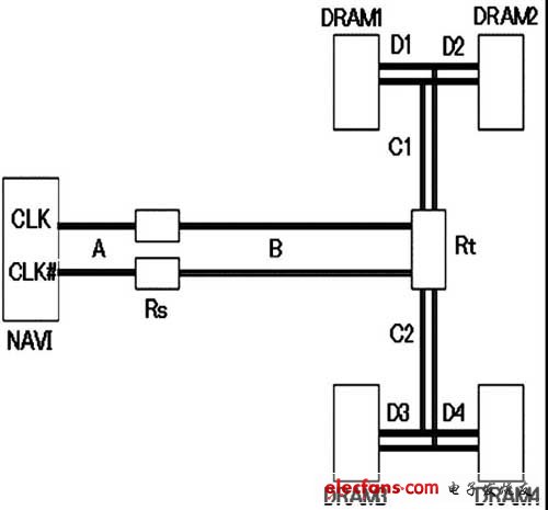
Figure 5 CLK wiring topology
As shown in Figure 6, the wiring topology map selected by the DATA group is indicated. The wiring points are as follows:
1 All DATA signals are from the NAVI-CPU to the length of each DRAM (ie A-B-C segment).
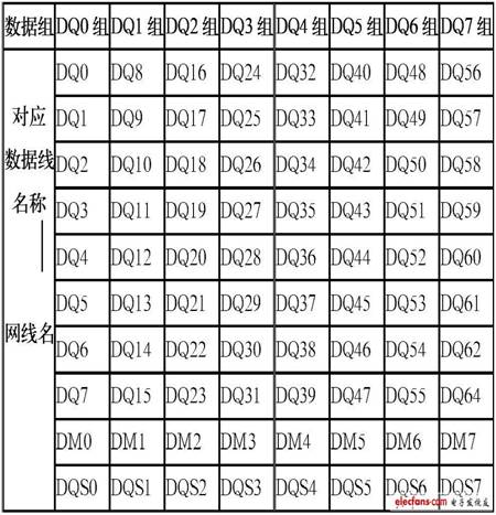
The error of 2 equal length wiring can be controlled by the error between the same Bit column and each group of bits, as shown in Table 2.
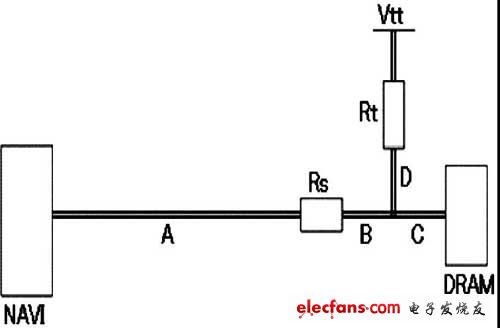
Figure 6 Layout of the DATA data group
Table 2
3.7 Address/Command wiring method
As shown in Figure 7, the wiring topology diagram selected for the Address/Command group is indicated. The wiring points are as follows:
1 The total wiring length (A - B - C - D ) is equal in length, and the length error between CLK and CLK is controlled within a certain range.
The wiring of the 2D segment (D1, D2, D3, D4) should be the same length.
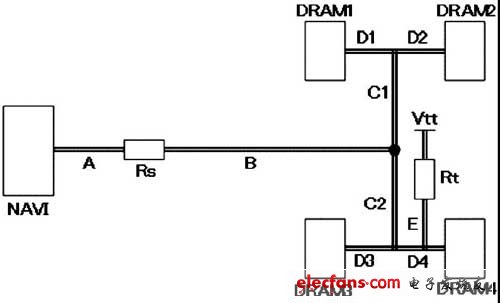
Figure 7 Routing topology diagram of the Address/Command data set
3.8 Design method for equal length wiring
In order to realize the equal length control of the network lines such as the DATA group and the Address/Command group, a wiring method (or a rectangular line) may be employed. However, if the length of the curve is too long or the width DM between the curves is too short, the signal transmission delay is shorter than the expected time due to the coupling between the electromagnetic fields, and is transmitted to the receiving end too early, causing the signal transmission to be unequal.
3.9 Power and Ground Wiring Methods
The power supplies used in DDR200 are 2.5V, 3.3V, Vref, Vtt, etc. The wiring points are as follows:
1Vref is used as the reference voltage for the input Buffer, and noise from other signals should be avoided. When wiring, pay attention to the coupling between the signals of the same layer and the coupling between the adjacent upper and lower layers. Also avoid mutual interference with Vtt (terminal voltage). Especially in the laminated structure of this example, attention should be paid to the effect of interlayer coupling with the CLK line of the third layer.
2 In order to reduce the trace impedance of Vtt and increase the wiring width as much as possible, it is recommended to lay the power supply surface.
4 Conclusion
Based on the working principle of DDR200, this paper introduces the PCB design method for realizing high performance of equipment. Nowadays, digital circuits have already seen higher speed DDR2 and DDR3. I hope that the design ideas of this paper and the wiring method of high-speed signals can help everyone's design.
LEDER offers a range of modern indoor illumination, including LED down light ,Track Light,Linear Light,indoor wall light,LED Panel Light,strip light,LED tube and bulbs as so on. Our indoor lights and indoor LED lighting solutions are ideal to create an atmosphere that is expected of LED lighting in commercial or residential Settings.
We believe in the aesthetics of indoor design and the role of lighting in enhancing the atmosphere of the indoor space, whether for entertainment or work. The indoor of the home is a place of relaxation, warmth and intimacy, while at work it is a place of creativity, efficiency and collaboration. The basic idea is that indoor space is an area where one can resonate with individuals or professionals and perform at their best. This is the importance of indoor lighting and the role of lamps and lanterns, they are used to enhance the space, bring the best results for the people who use the space. Modern Spaces may be limited by light, and sometimes the use of light in indoor Spaces during the day is almost inevitable. LEDER indoor lighting is by using the method of people-centered, applicability in lighting design and play out the best effect, make the person can achieve the best results in indoor space.
Indoor Lighting
Grow Lamp ,Indoor Grow Lighting ,E27 Indoor Wall Light,Indoor Motion Sensor Light
JIANGMEN LEDER LIGHTING CO., LTD , https://www.lederlight.com