IGBT is the core device of energy conversion and transmission. It is commonly known as the “CPU†of power electronic devices. As a strategic emerging industry, it is widely used in rail transportation, smart grid, aerospace, electric vehicles and new energy equipment.
As shown in the figure below, an N-channel reinforced insulated gate bipolar transistor structure, the N+ region is called the source region, and the electrode attached thereto is called the source (ie, the emitter E). The N base is called the drain area. The control region of the device is the gate region, and the electrode attached thereto is called the gate (ie, gate G). The channel is formed next to the boundary of the gate region. The P-type region (including the P+ and P-regions) between the C and E poles (the channel is formed in this region) is called a Subchannel region. The P+ region on the other side of the drain region is called a drain injector. It is a unique functional region of the IGBT. Together with the drain region and the sub-channel region, a PNP bipolar transistor is formed to function as an emitter. The drain injects holes and conducts conductive modulation to lower the on-state voltage of the device. The electrode attached to the drain implant region is referred to as the drain (ie, collector C).
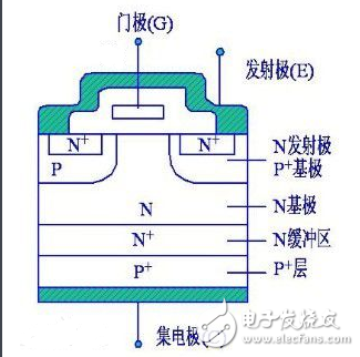
IGBT structure diagram
The switching function of the IGBT is to form a channel by adding a forward gate voltage, and provide a base current to the PNP (formerly NPN) transistor to turn on the IGBT. Conversely, the reverse gate voltage is applied to eliminate the channel, and the base current is cut off to turn off the IGBT. The driving method of the IGBT is basically the same as that of the MOSFET, and it only needs to control the input pole N-channel MOSFET, so it has high input impedance characteristics. When the channel of the MOSFET is formed, the hole from the P+ base is injected into the N-layer (small sub-), and the N-layer is conductance modulated to reduce the resistance of the N-layer, so that the IGBT also has a low voltage at a high voltage. On-state voltage.
Material parameters of IGBT moduleCurrently, power devices and modules use wire bonding interconnection processes and planar package structures. Figure 1 is an anatomical view of a conventional IGBT module.
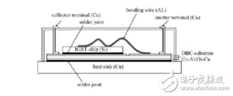
Figure 1 Schematic diagram of IGBT module structure
As can be seen from the above figure, the IGBT module consists of a total of seven layers, which can be roughly divided into three parts: chip, DBC and substrate. Each part is made of solder joints. This paper knows that IGBT is developed on the basis of thyristor, but compared with the traditional thyristor, the IGBT module eliminates the internal cathode and anode metal layers, which are replaced by the bonding wires drawn from the chip surface and the upper layer of DBC copper. In addition to this, the original nickel metal buffer layer was also removed at the expense of a reduction in the capacity of a single IGBT chip. In order to make up for this defect, this paper needs to place more IGBT chips on the DBC board [8].
IGBT modules are composed of different layers of materials, such as metals, ceramics, and high molecular polymers, as well as silica gels that are built into the module to improve the thermal properties of the device. Their thermal expansion coefficient and thermal conductivity are very different, and unexpected problems may occur during the operation of the device.
Physically, thermal conductivity represents the amount of thermal conductivity of an object. In the IGBT module, the thermal conductivity of the material involved is plotted as a column chart as follows:
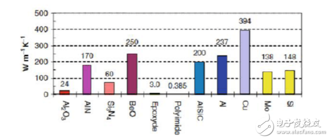
Figure 2 material thermal conductivity column chart
The coefficient of thermal expansion (CTE) refers to the change in volume of an object at a unit temperature, and its international unit is K-1. For a power device with a stacked structure such as an IGBT, the temperature is high under normal operation, and therefore different materials may also undergo different degrees of deformation due to the principle of thermal expansion and contraction, thereby affecting the reliability of the device. Figure 3 depicts the thermal expansion coefficients of several materials in the module.
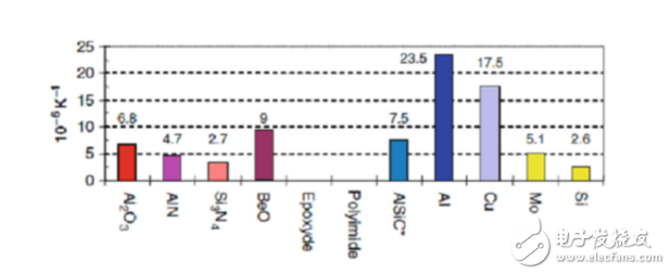
Figure 3 material thermal expansion coefficient
The introduction of organic materials can prevent the bonding wires from being corroded and have a high breakdown field strength. However, the organic film formed inside the module generates a large parasitic capacitance, which in turn affects some of the performance of the device.
In addition to the choice of materials, in fact, the thickness of each layer of material inside the IGBT module has its specifications. In the traditional IGBT module, the main component of ceramic is Al2O3, and the substrate is made of copper. In the high voltage IGBT module, the ceramic in DBC is replaced by AlN. Later, the high voltage IGBT module is improved. The main change is the use of silicon carbide aluminum. Replace the original copper substrate.
Table 1 Thickness of each layer of different IGBT modules: mm
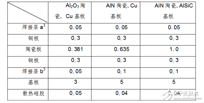
Of course, in certain cases, the required material thickness of the IGBT module is also different. For example, the original DBC ceramic thickness is 0.63mm, but in order to reduce the thermal resistance of the device, the later design size is 0.38mm; and for some IGBT modules that need to withstand higher voltage, the thickness of the internal aluminum nitride ceramic reaches 1mm.
LED Laser lamp,Full color led laser lamp
Kindwin Technology (H.K.) Limited , https://www.ktlleds.com