If you want to save the recordings in digital form, you should convert the analog recording signals into digital data, which brings a lot of inconvenience to the preservation of the original data. Therefore, the author designed a digital recorder according to the G.723 standard, which uses the ADSP-2181 as the voice processor and system controller, cancels the mechanical part and tape of the ordinary recorder, and uses a large-capacity flash memory (Flash RAM). As a digital voice data memory. The prototype is small in size, long in recording time, and has no mechanical noise and mechanical failure, which is very practical. 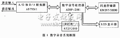
This article refers to the address: http://
The G.723 algorithm has a good codec effect on speech signals, and can also process music and other sound signals. The typical input is 64kb/s (8k%26; #215; 8) or 128kb/s (8k%26; #215;16) A-law or μ-law PCM sampled speech signal. Each time a frame of speech signal is processed, 240 samples per frame (30ms). At a code rate of 5.3 kb/s, each frame of speech is compressed into 20-byte transmissions; at a code rate of 6.3 kb/s, each frame of speech is compressed into 24 bytes of transmission.
1.2 Digital recording system structure block diagram The system block diagram is mainly composed of five parts as shown in Figure 1. 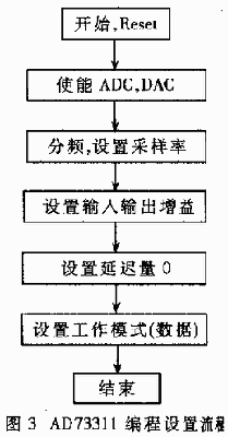
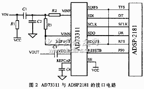
The AD73311 is a programmable data converter that contains five 8-bit control registers, CRA to CRE, for setting the operating state and controlling the input and output. The AD73311 interfaces with the processor through the serial port and transmits 16-bit data. There are five working modes: program mode, data mode, mixed mode, analog loop mode, and digital loop mode. The first three are normal working modes, and the latter two are debugging modes, which are only used during debugging. The five operating modes are controlled by four bits (CRA0~3) in the internal control register A.
Program mode: After the AD73311 is started or reset, it will work in program mode. At this time, the data input by the AD73311 serial port will be used as the command word to initialize the internal control register group. After that, the AD73311 enters the corresponding working mode according to the initialization command word. The code word output by the AD73311 serial port is invalid. Data mode: At this time, the AD73311 serial port outputs 16-bit data converted by A/D, and the input 16-bit data of D/A conversion. Once the AD73311 enters the data mode, it can no longer get control information, so it will always be in this mode unless restarted. At this time, the transmission and reception frame synchronization signal synchronization mode can be adopted on the hardware. Mixed mode: At this time, the 16-bit codeword may be a control word or data. The MSB of the codeword is used to identify whether the codeword is a control command word (MSB = 1) or data (MSB = 0, the lower 15 bits are valid data). In the hybrid mode, the ADSP-2181 can change the operating parameters of the AD73311, such as the amplification factor of the amplifier, according to the operating conditions of the system. At this time, the hardware can adopt the asynchronous method of transmitting and receiving the frame synchronization signal, which is convenient for the autonomous control of the ADSP-2181.
The AD73311 controls the sampling rate by the clock divider circuit. The clock divider circuit divides the external clock frequency MCLK input from the DMCLK pin into the internal clock frequency DMCLK by the main frequency clock factor. MCLK has five kinds of frequency selection, and is controlled by three bits CRB4~6 in the internal control register B. The DMCLK determines the sampling frequency of the AD73311, which is also the frame synchronization frequency of the AD73311 serial port. The DMCLK is divided by the serial clock division factor into the serial clock frequency SCLK. The DMCLK has four options, which are controlled by two bits of GRG2~3 in the internal control register B.
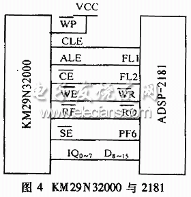
 The gain of the input and output can be controlled by programming control register D. The input gain IG can be adjusted between 0 and 38 dB, and the output gain OG can be adjusted between -15 and 6 dB. The specific programming flow chart of AD73311 is shown in Figure 3. The control program is as follows: AX0=DM(0x3fe5); {For 2181-PF0 connect with AD73311-RESET} AR=AX0 AND 0XFFFE; {PF0 pin reset} DM(0x3fe5)= {RESET AD73311 to program} NOP; {Delay} NOP; NOP AX0=DM(0x3fe5); AR=AX0 or 0X0001; {2181-PF0 SET} DM(0x3fe5)=AR; {ready to program} ax0=0x82f9 {Write control register CRC, 5V power supply, enable ADC and DAC} tx0=ax0; IDLE; ax0=0x811b; {write control register CRB, divide, set 8K sampling rate} tx0=ax0; IDLE; ax0=0x8320; {Write control register CRD, output input gain is 0} tx0=ax0; IDLE; ax0=0x8400; {write control register CRE, DAC delay is 0} ax0=ax0; IDLE; ax0=0x8001; {write control register CRA, Enter data transmission mode} tx0=ax0; IDLE; 2.2 Flash memory and ADSP-2181 interface circuit Flash memory adopts KM29 N32000 produced by Samsung, Korea, with a capacity of 4M%26; #215;8=32Mbit, divided into 512 blocks Each block has 16 pages and 528 bytes per page. It can perform 1 million erasing and writing, and the data storage time is 10 years. It can be automatically erased by programming. This is used to save the recorded data, and its data is saved without charge maintenance.

3 System Control Software Design The ADSP21XX series provides a complete set of software development tools and corresponding simulator development platform, which provides great convenience for system debugging and simulation. The software development system includes a system builder, a C compiler with a runtime time library, an assembler, a connector, a PROM partitioner, and the like. An EXE file can be generated by compiling the assembly source program. This file is a storage image file that can be loaded onto the emulator for simulation. After successful debugging, the EPROM can be written to the EPROM by the PROM divider and the EPROM burning device. When the system is reset, the DSP can be automatically loaded by the EPROM program to control the entire system. jobs. The system software design adopts two methods: bootstrap and interrupt control. When the bootstrap mode system is powered on, the ADSP-2181 reads the programs in the EPROM and automatically runs the program to control the entire system.
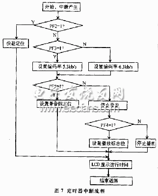
Interrupt control utilizes two interrupts of the ADSP-2181, namely the sport0 receive interrupt and the timer interrupt. The ADSP-2181's sport is connected to the AD73311. When a sampled data is obtained, a receive interrupt is generated, and the ADSP-2181 reads the sampled data. Since sport0 is full-duplex, when the reception interruption occurs, data can be sent at the same time. On the one hand, the playback effect can be obtained during recording; on the other hand, the data can be directly transmitted during playback, and the sampled data is ignored, which is convenient for decoding. The data is played back at a fixed code rate. Timer interrupt timing detects the status of the external control pin, including recording, playback, fast-release and rate conversion. 4 pins, the 0/1 status of each pin corresponds to two kinds of control, that is, start recording/stop recording, start to put Sound/stop playback, 5.3kbps/6.3kbps rate conversion and fast release status, there are seven states. The structure of the DSP assembly language is similar to the ASM assembly language, and the beginning part corresponds to the interrupt vector table. When working in the interrupt mode, the vector table corresponding to the interrupt is generally a jump statement; when an interrupt is generated, it jumps to the corresponding statement to execute the interrupt control function. The interrupt settings of the main program are as follows: JUMP start; NOP; NOP; NOP; {reset start interrupt} RTI; NOP; NOP; NOP; {IRQ2} RTI; NOP; NOP; NOP; {IRQL1} RTI; NOP; NOP; NOP;NOP;NOP; {sport0 receive} RTI;NOP;NOP;NOP; {IRQE} RTI;NOP;NOP;NOP; {BDMA} RTI;NOP;NOP;NOP; Sport1 transmit} RTI;NOP;NOP;NOP; {sport1 receive} JUMP settimer;NOP;NOP;NOP; {timer interrupt} RTI;NOP;NOP;NOP; {PowerDown} The sporto and timer interrupt control are described as follows: (1) The sporto receives the data interrupt in the program, and the data processing is concentrated here. The main process is: G.723 encoding is performed every 240 samples of data received during recording, and the encoded result is saved to the flash memory; during playback, 24 data is read each time, and the data will be read. Decoded, then sent out through the serial port, and restored to a voice signal through the speaker. The process is shown in Figure 6. (2) The timer interrupt timer interrupt is used to detect the user's control information and display the running time information. There are 4 user controls, namely rate selection, recording control, playback control and fast reverse control. Corresponding to these four control pins, the initial setting is the input state, and then the operating state is set by detecting the level of each pin. The process is shown in Figure 7.
4 System debugging system debugging should use the complete software development tools and simulators of ADSP21XX series provided by AD company. I use the ADSP-2181-EZ-ICE simulator for debugging. The simulator comes with 33MHz of 33MHz. The debugging supports 20 breakpoints. It can be single step, set breakpoint and run at full speed. You can observe and modify the values ​​of registers and storage units at any time. A 14-pin emulation interface is provided on the emulator, through which the emulator simulates the target system. There is an RS-232 interface between the emulator and the computer, which is connected to the serial port of the computer through data, and software debugging can be performed on the emulator development platform. The main problems encountered during system debugging are memory read and write and LCD display problems. Initially, it was found that the data written into the flash memory did not match the data read. After careful analysis, it is found that the programming is not strictly in accordance with the read/write operation timing of the flash memory, or the delay amount is not enough, or the order of the two signals is reversed, the data may not be written at all, and the read data is not read. Of course it is wrong. After the program control is strictly performed according to the timing of the specification, the data read/write erase operation is completely normal. When playing the recorded data, there was a problem that the sound jump was discontinuous. After analysis, the reason was that the address was wrong. Because each time the read and write of the flash memory is one frame of data, and the data of one operation at the time of encoding and decoding is 20/24 bytes, the length of the two is different, and the conversion operation is required.
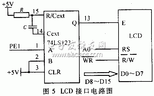
The machine cycle of the ADSP-2181 processor in this system is 30ns, and the maximum waiting period is set to be 24ns after 7 machine cycles, and the LCD has a working enable pulse width of at least 300ns. Therefore, a monostable delay circuit is added to the hardware, which solves this problem.
Double Wall Electric Water Boiler Urn
Double wall electric water boiler urn
Double wall electric water boiler urn
FOSHAN FORTUNE ELECTRICAL APPLIANCE CO.,LTD , https://www.coffelady.com