One significant change in the specifications of different power converters is the need to convert a wide range of input voltages into regulated output voltages. However, if the unregulated input voltage is constantly changing above, below, or equal to the set point of the regulated output voltage, this task will change when buck-boost conversion is required. It is even more challenging. Buck-boost conversion is essential for a wide range of applications, including battery charging, solid state lighting, industrial computing, and automotive applications.
This article briefly reviews many of the factors associated with a 4-switch buck-boost converter design. Specifically answer questions about component selection and power calculations, and use the Quick Start Calculator tool to coordinate and speed up the converter design process.
Synchronous Buck-Boost Converter Operation
As an effective way to provide both boost conversion and buck conversion, a well-designed buck-boost circuit becomes an indispensable device due to its convenience. Let's review the 4-switch (non-reverse) synchronous buck-boost topology shown in Figure 1.
The main advantage of the buck-boost power stage is that the buck, boost, and buck-boost conversion modes achieve high efficiency over a wide range of input and load currents as needed. It also provides a positive output voltage compared to a similar single-switch (reverse) buck-boost, as well as lower power relative to SEPIC, flyback, and cascading boost-blow topologies. Loss and higher power density.
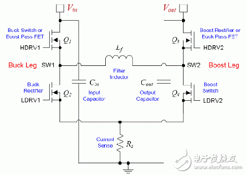
Figure 1. 4-switched synchronous buck-boost converter power stage.
In Figure 1, four power MOSFETs are arranged as buck and boost bridge arms in an H-bridge configuration where switch nodes SW1 and SW2 are connected by an inductor LF. When the input voltage is higher or lower than the output voltage, respectively, the synchronous buck or boost starts to run, while the high-side MOSFET of the opposite non-switching bridge arm operates as a conducting device. More importantly, when the input voltage is close to the output voltage, the switching buck or boost bridge arm reaches the expected duty cycle limit, triggering a transition to the buck-boost mode of operation. Changes in operating mode should be smooth and autonomous, without changing the control configuration. The way this is achieved, and the possible interdependencies between power levels and control mechanisms, is very important.
For example, as a specific buck-boost controller, the LM5175[4] uses a unique mechanism in buck-boost mode with buck and boost bridge arms in a quasi-interleaved manner at reduced frequencies. Switching, which has significant advantages in terms of efficiency and power loss. Peak current mode and valley current mode buck control technology enable smooth and smooth mode conversion, requiring only a low-side configured voltage divider resistor for current sensing. The slope compensation implementation based on the difference between VIN and VOUT is often a deadbeat response and is a good way to increase power supply rejection (PSR) and suppress line transients.
Design flow for current mode buck-boost converter
Figure 2 shows a complete circuit schematic of a 4-switch synchronous buck-boost converter. This schematic includes components for the power stage, the bootstrap circuit of the gate driver, the current sensing network, and spread spectrum frequency modulation (SSFM) for lower electromagnetic interference (EMI), [5] programmable Components for undervoltage lockout (UVLO), output feedback, and loop compensation.
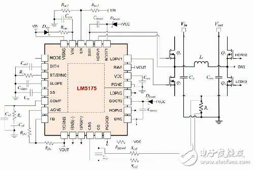
Figure 2. Schematic of the 4-switch buck-boost converter with current mode controller.
A fast start tool resource [3] provides an analysis and design framework for a 4-switch buck-boost converter. The steps are from converter specification to component selection to performance verification (efficiency, component dissipation, and Bode plot), and if necessary, repeat design. Taking the LM5175 synchronous buck-boost controller as a starting point, let's review the design flow of the 400kHz converter step by step; this converter provides a 6A to 42V input voltage at 6A rated current. 12V output.
Nickel Iron Battery,Nickel Iron Alkaline Battery,Solar Battery,Nickel Iron Battery For Solar
Henan Xintaihang Power Source Co.,Ltd , https://www.taihangbattery.com