Opening an electronic device is easy for an end user; just press the button. However, it takes a lot of effort to create a smooth and smooth power-up experience. Excessive system switching will result in a power failure caused by an uncontrollable inrush current spike. For microprocessor or FPGA based applications, proper operation requires a specific power rail sequencing. Sometimes it is best to power up a particular subsystem before enabling downstream circuitry. Using load switches to manage power sequencing makes it easier for end users to have a smooth, smooth power-up experience.
In most systems, capacitors are placed throughout a design to ensure that there is no power rail voltage drop. At the beginning of power up, charging these capacitors will result in an inrush current; this inrush current will exceed the maximum current rating of the downstream circuit. If left unchecked, this will put the voltage rail out of regulation, putting the system into an unfavorable state. Failure to inspect and limit inrush current can also damage board connectors and board traces because inrush currents exceed their load carrying capacity. In order to manage the inrush current, the voltage applied to the capacitive load needs to have a controlled rise time. All Texas Instruments (TI) load switches have an integrated soft start, and some devices even offer adjustable rise times for varying capacitive loads. Figure 1 shows this integrated soft start.
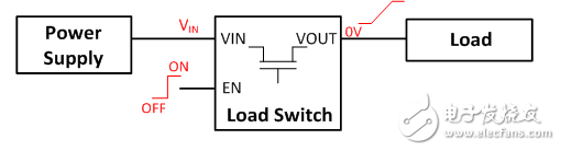
Figure 1: A load switch that provides controlled rise time for system load
Placing a load switch between the power supply and the capacitive load can greatly reduce the inrush current when the load is turned on/enabled. Many processors and FPGAs have very specific power sequencing requirements, as well as a specific power rail turn-on sequence. The load switch makes it easier to meet power sequencing requirements, enabling point-of-load control for each rail. Then, powering each rail is as simple as sending the correct GPIO signal to the correct load switch. Figure 2 shows this concept.
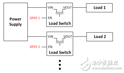
Figure 2: Power sequencing using separate GPIOs for each load
Some load switches even have a power good (PG) signal; this signal indicates when the output is fully turned on. By connecting the PG signal to the enable pin of the next load switch in the sequence, the power sequencing requires only one GPIO signal for all power rails. Figure 3 shows this configuration.
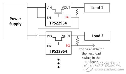
Figure 3: Power sequencing without GPIO signals
The load switch is also effective for system power down. The fall time of the load switch is determined by the discharge speed of the output load to its capacitor. To speed up this discharge process and ensure a 0V state, some load switches have a fast output discharge (QOD) characteristic, as shown in Figure 4, which discharges the output to ground through an internal resistor.
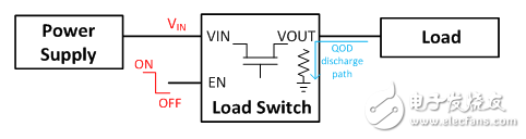
Figure 4: A load switch that supports QOD
Whether the system is powered or discharged, the load switch makes timing and sequencing requirements as simple as pressing a button.
Zigbee Compatible Bulbs,Zigbee Flexible Smart Bulb,G-Series Zigbee Light Bulb,Zigbee Filament Bulb
t-smartlight , https://www.t-smartlight.com